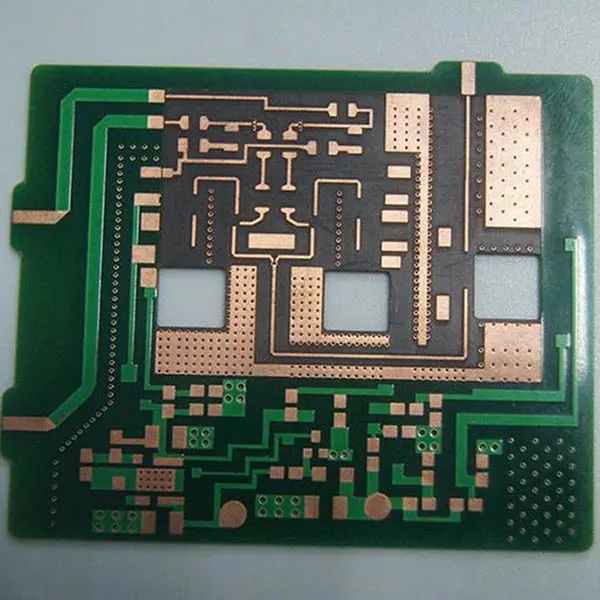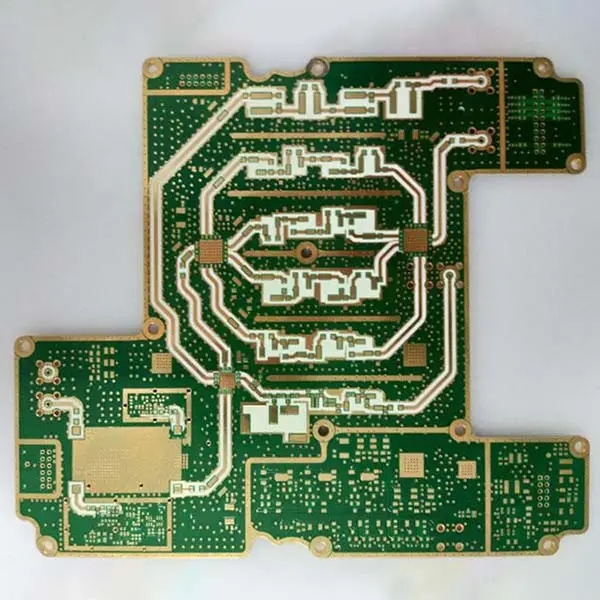
Detailed explanation of special PCB processing methods you don't know
Laser Direct Imaging
Instead of exposing the plate with negative film for image transfer, the computer commands the laser beam to directly conduct rapid scanning photosensitive imaging on the dry film. As a single beam of concentrated parallel light is emitted, the side wall of the dry film after imaging can be more vertical. However, the method can only work on each plate separately, so the mass production speed is far faster than using negative film and traditional exposure. LDI can only produce 30 medium-sized boards per hour, so it can only occasionally appear in prototype proofing or high price boards. Due to the high congenital cost, it is difficult to promote in the industry.
Laser Maching
In the electronic industry, there are many precision processes, such as cutting, drilling, welding, welding, etc., which can also be carried out with the energy of laser light, called laser processing. The so-called LASER refers to the abbreviation of "Light Amplification Stimulated Emission of Radiation", which is translated by the mainland industry as "laser", which seems more relevant than transliteration. Laser was produced by T.H. Maiman, an American physicist, in 1959 by projecting a single beam of light onto a ruby. Over the years, research has created a new processing method. In addition to the electronic industry, it can also be used for medical and military purposes.
Micro Wire Board
The round section enamelled wire (sealant wire) attached to the board surface is made into a special circuit board with PTH to complete inter layer interconnection. It is commonly known in the industry as the Multiwire Board "double wire board". When the wiring density is very large (160~250 in/in2) and the wire diameter is very small (less than 25 mil), it is also called the micro sealed circuit board.
Moulded Circuit
The stereo die is used to complete the manufacturing process of the stereo circuit board by injection molding or transformation, which is called Moulded Circuit or Moulded Interconnection Circuit. The left figure is the schematic diagram of the MIC completed by two shots.
Multiwiring Board (or Discrete Wiring Board)
It refers to the multilayer interconnection circuit board, which is obtained by using extremely thin enamelled wires to directly cross connect the copper foil free board, then coating, fixing, drilling and plating holes. It was developed by PCK, an American company, and is still being produced by Hitachi, a Japanese company. This kind of MWB can save design time, and is suitable for a small number of models with complex circuits (there is a special article in the 60th issue of the Journal of Circuit Board Information).
Noble Metal Paste
It is conductive printing paste for thick film circuit printing. When it is printed on the porcelain substrate by screen printing, and the organic carrier is burned away at high temperature, a fixed precious metal circuit appears. The conductive metal powder added to the printing paste must be precious metal to avoid the formation of oxides at high temperatures. The commodities are used for gold, platinum, rhodium, palladium or other precious metals.
Pads Only Board
In the early through-hole insertion era, in order to ensure the solderability and circuit safety of some high reliability multilayer boards, only the through-hole and the solder ring were left outside the board, while the interconnecting circuits were hidden on the next inner layer. This kind of board with two more layers will not be printed with solder proof green paint, and the appearance is particularly exquisite, and the quality inspection is extremely strict. At present, due to the increase of wiring density, many portable electronic products (such as cell phones) have only SMT pads or a few lines left on their circuit boards, and many of the interconnecting dense wires are buried in the inner layer. The layers are also changed to use highly difficult blind holes or "Pads On Holes" as interconnections to reduce the damage of the full hole to the ground and the copper surface with high voltage. This SMT flush mounting board is also the only type of pad.

Polymer Thick Film (PTF) thick film paste
It refers to the precious metal printing paste used for manufacturing circuits of ceramic based thick film circuit boards, or printing paste used to form printed resistance films. Its manufacturing processes include screen printing and subsequent high-temperature incineration. After burning off the organic carrier, there will be a firmly attached circuit system, which is commonly referred to as Hybrid Circuits.
Semi Additive Process
It refers to the process of directly growing the required lines on the insulating substrate surface in the form of chemical copper, and then continuing to thicken them in the form of electroplated copper, which is called "half addition". If chemical copper method is adopted for all line thicknesses, it is called "full addition" process. Note that the above definition is from the latest specification IPC-T-50E issued in July 1992, which is different from the original IPC-T-50D (November 1988). The early "version D" and the industry's general statement refer to the bare non-conductive substrate or the substrate with thin copper foil (such as 1/4 oz or 1/8 oz). First prepare the image transfer of negative resistor, and then thicken the required circuit by chemical copper or copper electroplating method. The new 50E does not mention the word "thin copper skin". There is a big gap between the two statements. It seems that readers should follow the times in their ideas.
Subtractive Process Subtraction
It refers to removing the useless copper foil on the surface of the substrate, and the method to achieve the circuit board is called "reduction method", which has been the mainstream of circuit boards for many years. It is the opposite of the other "addition method" of directly adding copper plated conductor lines on copper free substrate plates.
Thick Film Circuit
The PTF thick film paste containing precious metal components is printed on a ceramic substrate plate (such as aluminum oxide) by screen printing, and then fired at high temperature to form a circuit system with metal conductors, which is called "thick film circuit". It belongs to a small "Hybrid Circuit" board. The "Silver Paste Jumper" on a single-sided PCB also belongs to thick film printing, but it does not need to be fired at high temperature. The lines printed on the surface of various base materials must be more than 0.1 mm [4 mil] thick before they are called "thick film" lines. The manufacturing technology of this "circuit system" is called "thick film technology".
Thin Film Technology
It refers to the conductor and interconnection circuit attached to the substrate. Where the thickness is less than 0.1 mm [4 mil], it can be produced by vacuum evaporation, pyrolytic coating, cathodic sputtering, chemical vapor deposition, electroplating, anodizing, etc., which is called "film technology". Practical products include Thin Film Hybrid Circuit and Thin Film Integrated Circuit.
Transfer Laminated Circuit
It is a new circuit board production method, which uses a 93 mil thick treated and smooth stainless steel plate to perform the pattern transfer of the negative film dry film first, and then high-speed copper plating of the circuit. After stripping the dry film, the stainless steel plate surface with lines can be pressed on the semi hardened film at high temperature. After the stainless steel plate is removed, the circuit board with flat surface and embedded circuit can be obtained. Later, holes can be drilled and plated to obtain interconnection between layers. CC-4 Copper complexer 4 ; It is the full addition method developed by PCK in the United States on the special copper free substrate (see the special article in the 47th issue of PCB Information Magazine for details) ED Electro - Deposited Photoresistor; Electric resistance IVH Interstitial Via Hole; MLC Multilayer Ceramic for local interlayer through holes (including buried through holes and blind through holes); Small porcelain multilayer circuit board PID Photoimagible Dielectric; Photosensitive medium (refers to the photosensitive plate coated by layer adding method) PTF Polymer Thick Film; Polymer thick film circuit boards (refer to thin film circuit boards printed with thick film paste) SLC Surface Lunar Circuits; The surface thin layer circuit is a new technology published by IBM Japan Yasu Laboratory in June 1993. It is a circuit with several layers of interconnections formed by Curtaining Coating green paint and electroplating copper on the outside of the double-sided plate. It is no longer necessary to drill and plate holes on the plate.
PCB manufacturers, PCB designers and PCBA manufacturers explain special PCB processing methods that you do not know.


