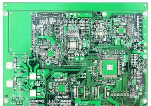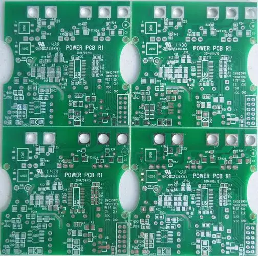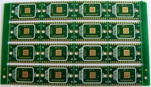
Conductive hole: via
Keyhole: pad

Several problems that are particularly prone to occur:
1) Mixed use of pad and via leads to problems
1) When your files are pads or protels, they are sent to PCB factories, and they require the vias to be covered with oil. Be careful. You should carefully check whether your plug-in holes (pads) are also useful for via, otherwise your plug-in holes will also be covered with green oil, which will lead to non soldering disputes: the plug-in holes must be coated with tin. How do you cover the oil and how do I use it? Please check the files when you say this, It is designed by pad or via!
2) When your file is pads or protel, send it to the factory. The order requires that the conductive hole be covered with oil. Many customers use pad (plug-in hole) to represent the conductive hole, which causes your conductive hole to open the window. Maybe you want the conductive hole to cover with oil. At that time, the point of dispute may be that I want the conductive hole to cover with oil. Why do you open the window? Please check your file design!
PCB design
PCB: This point has been repeatedly emphasized. If you are a via, you will be treated as a via. If you are a pad, you will be treated as a pad! Because no one will know that you are a conductive hole, that is a plug-in hole, and via and pad are the only marks,
2) Via In the conversion process, problems occur due to non-standard design or unclear rules for gerber conversion
3) When you send a gerber file, the pcb proofing factory can't tell which are vias and which are keyholes. The only thing that can be identified is processing according to the file. If there is a welding flux layer, there is a window! Argument point: I asked for a hole covered with oil. Now you open the window for me. I may cause a short circuit. Please check your file. Your gerber is a film file. The factory has no way to check your conductive hole or keyhole. Please check the gerber file. If there is a soldering layer, open the window. If not, cover with oil
3: How to design via cap oil in protel or pads------ This is the most standard practice. If the design is standard, there will be no mistakes!
There is a tenting option in the via attribute of protel. If it is checked, it must be oil capping. Then all the oil you transfer out is oil capping. In pads, the way to transfer files from pads is to think about hole (via) oil capping:
When outputting soldermask, that is, PCB solder mask, just check the upper soldermask top ---- the lower vias, which means that all vias are windowed. If not checked, the vias are covered with oil
To sum up:
The pad is made according to the pad. This is the plug-in hole. Via, you have two choices. If you provide the original file, you can choose it when placing an order. If you provide the gerber file, you must check whether the gerber file meets your requirements!


