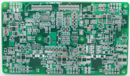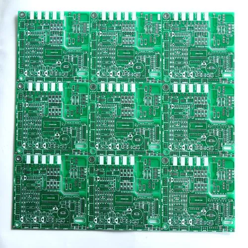
PCB, also known as PCB, is an important electronic component, the support of electronics, and the provider of electrical connection of electronic components.
PCB proofing refers to the trial production of printed circuit boards before mass production. It is mainly applied to the process of small batch trial production of electronic engineers to the factory after the completion of circuit board design. However, there is no specific limit for the production quantity of PCB proofing. Generally, engineers call it PCB proofing before the product design is confirmed and tested.
2、 Focus of proofing
1. Speed
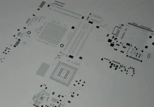
The products in PCB market change all the time. Time is a very important factor in this industry. Delivery time and quality are the hard strength of the factory, and are also the most favored by engineers and factories. At present, PCB factories generally provide urgent service, and the normal delivery time of fast manufacturers is also two days. For example, in Jingbang Electronics of Guangming, by default, all samples are monitored in real time during the whole process of expediting, quality control, engineering and production. Our advantage lies in the advanced production equipment: MYDATA-600, which eliminates the need for steel mesh, automates production, saves time and effort, and is a precision product.

2. Quality
It is the trial production of engineers before the confirmation and testing of product design is completed, and the quality cannot be ignored. From raw materials, drawings, production links, inspection, quality control, etc., each link needs to be strictly controlled. For example, for ordinary double-sided panels, the panel materials generally include FR-4, aluminum substrate, CEM-1, etc. The thickness of the panels ranges from 0.4mm to 3.0m, and the copper thickness ranges from 0.5oz to 3.0oz. The difference in these materials results in a great difference in the quotation. At present, the manufacturers use imported profit producing panels as the better materials.
3. Price
With the development of the industry, the price of medium and small batch production is declining. At present, many proofing companies, such as Jiepei, have cancelled all proofing/small batch film fees, and film fees have withdrawn from the historical stage. Complete challenging tasks with challenging prices. This will be the price trend of PCB proofing.
3、 Measurement standard of PCB proofing quality
1. The copper sheet is not easy to fall off under high temperature;
2. The line thickness, line spacing and line width of the line shall meet the design requirements to prevent heating, short circuit and open circuit of the line;
3. PCB circuit board has no additional electromagnetic radiation;
4. During PCB proofing, high temperature, high humidity and other special environments are considered;
5. Copper surface is not easy to be oxidized; The service life of oxidized circuit boards will be greatly shortened.
6. Reasonable deformation error; Nowadays, mechanical installation is adopted, and the hole position of the circuit board and the deformation error of the circuit design should be within the allowable range.
Combining the above six aspects to measure the printed circuit board, we can judge whether it is "excellent" or not. At present, there are tens of thousands of PCB manufacturers in the market. It is recommended that users should be careful in the selection process, and select manufacturers based on a certain understanding of PCB to prevent being deceived.
At present, the demand group for PCB proofing is mainly concentrated in the regions where electronic products are relatively developed, mainly including Shenzhen, Beijing, Shanghai, Suzhou, Hangzhou, Xi'an, Chengdu, Changsha and other cities. However, with the gradual maturity of China's PCB industry, the growth rate of the industry tends to be stable, and the domestic PCB industry is undergoing structural changes. The market share is biased towards excellent PCB manufacturers, and the industry concentration is expected to further improve.
For those who invest in this area, we have seen the points and cost calculation methods of patch processing.
The current product processes mainly include: lead-free welding process, lead welding process and red glue welding process. However, many users do not know how to calculate the points and costs of SMT patches. Today's small editor specially shares the points and cost calculation method of SMT chip processing:
Some companies count one pad as a point, but others count two pads as a point. This paper takes pad calculation as an example. It is only necessary to calculate the number of all pads on the PCB, but for some special components, such as inductance, large capacitance, IC, etc., the demand rating is calculated. The detailed experience method is as follows: for example, inductance can be counted as 10 points, and IC is folded in half according to the number of pins (for example, 40 pin IC, counted as 20 points). According to the above method, the total number of solder joints of the entire PCB can be easily calculated.
PCB proofing
2、 Unit price of solder joint:
At present, the unit price of solder joints varies from 0.008 yuan to 0.03 yuan per solder joint, depending on the following conditions:
1. Unit price according to process:
A Solder paste with lead SMT chip processing price is relatively cheap.
The processing cost of lead-free SMT pastes of solder paste B is relatively high.
The processing cost of C red glue environmental protection SMT patch is relatively low.
D solder paste red glue dual process SMT patch processing cost is high, the process is relatively troublesome.
2. Quantity by order:
A For 3 to 20 pieces of common SMT chip proofing processing, the engineering fee will be charged, and it will not be calculated by multiplying the points by the unit price.
B For small batch SMT chip processing and production of less than 1000 pieces, the startup fee+points multiplied by the unit price will be charged.
C Batch SMT chip processing, calculated by multiplying the number of points by the unit price.
3. According to the difficulty of the board
A Single sided SMT patch processing is relatively fast, while double-sided SMT patch processing needs to be switched to twice, which is costly.
B Precision SMT chip processing. Solder pastes for BGA high-density IC boards will be expensive.
C The density of SMD components is divided into many points in PCB boards of the same size. The efficiency will be high, because the travel of the coordinates is short when the SMT mounter is working, the faster the SMT chip processing will be.
4. Start up fee: small batch processing orders with single batch and single processing fee less than 1000 yuan. For small batch SMT chip processing orders, after counting the number of points, depending on the type of board sub components and the time of debugging the chip mounter, a start-up fee ranging from 400 to 2000 yuan will be charged depending on the difficulty of making the first piece.
5. Proofing fee: SMT chip processing orders with less than 100 pieces are SMT chip proofing orders. The difficulty of the board, the time to do the program, and the time to go on the machine and transfer to the line are different, so the engineering fees ranging from 800 yuan to 3000 yuan will be charged.
6. Steel mesh fee: open different models of steel mesh according to the size of PCB. According to the precision of the chip on the PCBA board, choose to turn on electric polishing steel mesh or ordinary steel mesh. The cost of different types of steel mesh is about 120~350. Of course, customers can also provide their own steel mesh.


