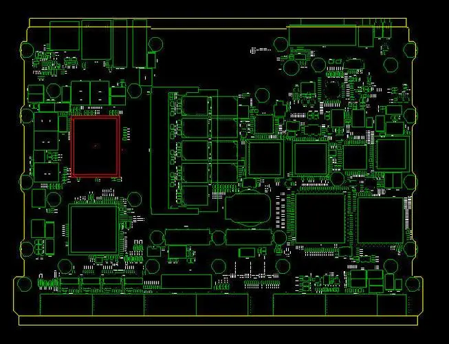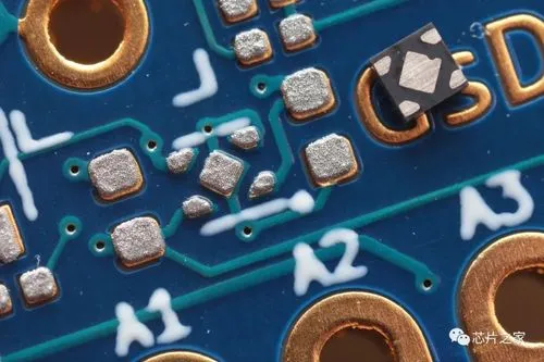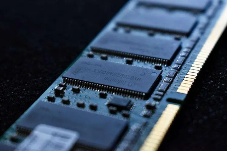
It is estimated that the printed circuit board industry will not be eliminated in the past 50 years. After all, all electronic products need to be used, even if they are small. Every line has many things that laymen do not know. There are many seemingly difficult but really simple, seemingly simple but very difficult processes. Today, I will reveal the production process of circuit boards to you.
PCB inserted with PCB components
There are many kinds of materials and PCB process flow for printed circuit board, and there are many kinds of materials alone, such as copper clad plate, ceramics, soft film, aluminum substrate, etc. Each material and requirement has different process flow. First, let's understand the simplest and most original process flow, ordinary process, Its production process is as follows: cutting - drilling - copper deposition (one copper) - circuit printing - electroplating (two copper) - etching - solder resistance printing - text printing - oxidation resistance (tin spraying, gold deposition, nickel deposition) - forming (gongs) - testing - shipping.

Our cutting process does not mean to cut directly according to the size of the finished product, but to design the cutting drawing and cut according to the most reasonable production size of the machine in a batch way. Factors such as cost utilization and convenience for production should also be considered. So drilling is to drill through the place where we need a hole. The hole actually serves as a conductive connection between the upper and lower parts. Some holes are also used for production positioning. Then enter the copper sink, which is mainly used to sink copper into the hole. Because the material is copper clad plate, it only has copper on the surface but not inside, so there is no copper in the hole. Without copper, there is no way to conduct electricity. After the hole is completed, the circuit is made, and a layer of circuit oil is brushed to show the circuit pattern through exposure. The second copper deposition is electroplating, which increases the thickness of copper and adds tin to distinguish the conductive line from the non conductive line. Enter the etching machine and disconnect the redundant copper surface from the non conductive line. Solder resistance oil is printed, and the welded points are also exposed. And print the words as marks, and finally do surface treatment, which is the process of oxidation resistance. At this point, our PCB is basically ready and can be connected normally. As long as we use gongs and machines to mill large production boards into finished boards required by customers, we can ship after passing the test.
The above is just a relatively simple and basic PCB manufacturing process. In fact, there is a lot of knowledge in the production process,
SMT small batch patch processing plant controls the quality of patch proofing
Now, with the rapid development of all walks of life and the demand for the rapid development of science and technology, electronic products have also been greatly developed, and SMT chip proofing processing has also developed rapidly. However, in this uneven industry, it is inevitable that there will be some enterprises that cannot guarantee the quality of SMT chip proofing processing. In fact, it is not advisable to sacrifice quality in exchange for low price processing. To be a processing enterprise, you must have the spirit of craftsmanship. A good board can not be all entrusted to good marketing, but rather the good processing quality of this PCBA board.
SMT chip proofing
How the processing factory controls the quality of SMT chip proofing processing. To control the processing quality of SMT chip, some necessary conditions should be met:
1、 Complete incoming material inspection and confirmation process to strictly control materials.
2、 The new model production project team checks the quality of new customers' first production.
3、 Nitrogen process and device storage should be applied to customers of pcba products with high requirements and high accuracy.
4、 SMT chip workshop environment monitoring: 25+/- 2 degrees, relative humidity: 40% - 60%.
5、 SMT auxiliary materials use high-quality solder paste to ensure the quality and stability of patch welding.
6、 Professional technical team, engineers/technicians have more than 10 years of working experience in smt industry.
7、 The equipment is a high-precision mounting machine, with the minimum mounting size of 0201, to ensure the SMT mounting accuracy and efficiency.
8、 Strict SOP production process control, SMT patch, DIP welding and back-end assembly test.
9、 10 temperature zone reflow welding is selected for reflow welding to ensure the quality of reflow stage, and various types of PCBA products should be handled.
10、 The first article confirmation process is rigorous, and the final version is confirmed together with the customer according to PCB drawings, PCBA samples, etc.
11、 Production process control: solder paste viscosity detection, solder paste printing thickness detection, chip mounting accuracy detection, furnace front mounting detection, regular spot check after the furnace, AOI full inspection after the furnace, and finished product detection.


