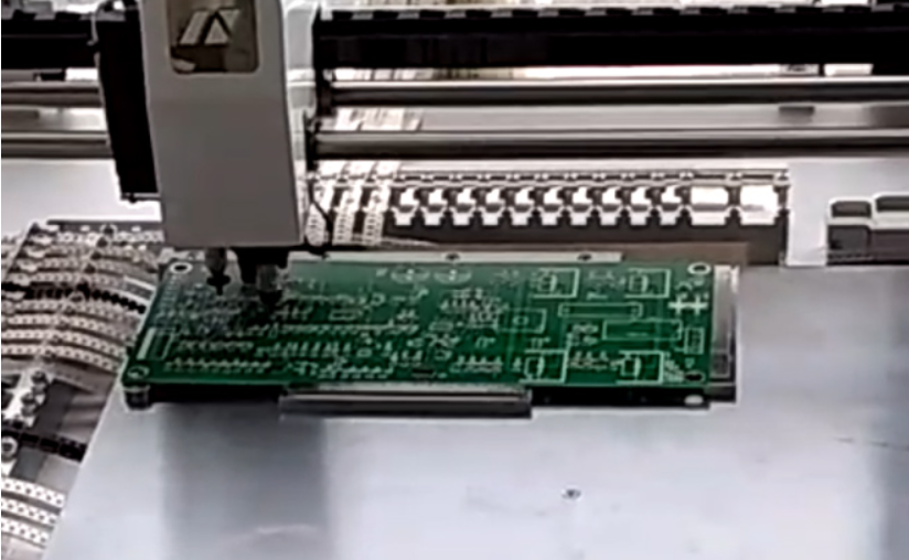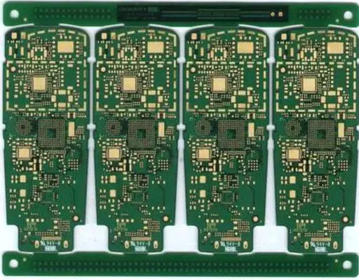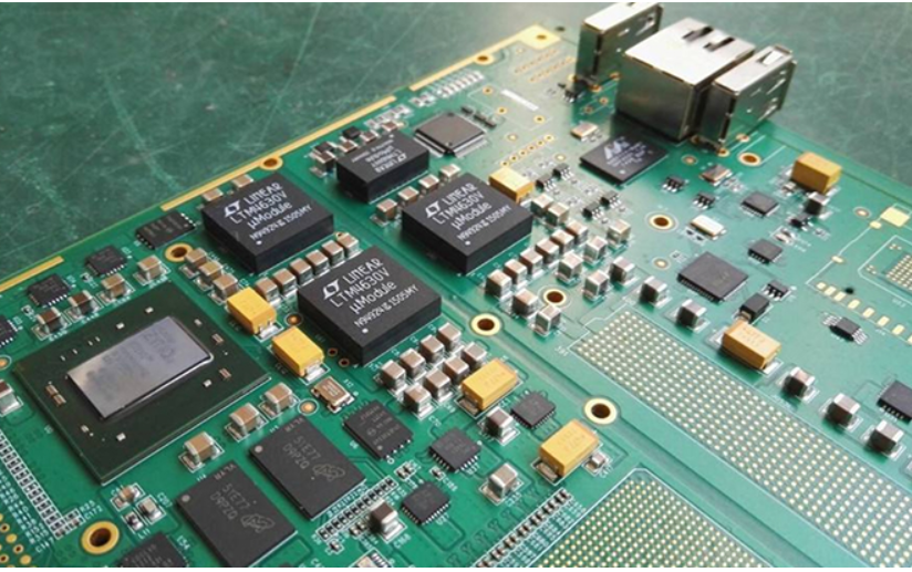
Land, the basic constituent unit of surface mount assembly, is used to form the land pattern of the circuit board, that is, various pad combinations designed for special component types. There is nothing more frustrating than a poorly designed pad structure. When a pad structure is not designed correctly, it is difficult, sometimes even impossible, to achieve the desired welding point. Pad has two words in English: Land and Pad, which can often be used alternately; However, functionally, Land is a two-dimensional surface feature for surface mountable components, while Pad is a three-dimensional feature for pluggable components.

As a general rule, Land does not include plated through hole (PTH). The bypass hole (via) is a plated through hole (PTH) for connecting different circuit layers. Blind via connects the outermost layer to one or more inner layers, while the buried bypass hole only connects the inner layer.
As noted earlier, pad Land in the PCB industry generally does not include plated through-hole (PTH). PTH in a pad Land will take away a considerable amount of solder during welding, and in many cases, solder joints with insufficient solder will be produced. However, in some cases, the wiring density of PCB design components is forced to change to this rule. The most noteworthy is the chip scale package (CSP). Below the 1.0mm (0.0394 ") spacing, it is difficult to route a wire through the" maze "of the pad. Blind bypass holes and micro via are generated in the pad, allowing direct routing to another layer. Because these bypass holes are small and blind, they will not absorb too much solder, resulting in little or no impact on the amount of solder at the solder joint.
There are many industrial documents out of IPC (Association Connecting Electronics Industries), EIA (Electronic Industry Alliance) and JEDEC (Solid State Technology Association), which should be used when designing pad structures. The main document is IPC-SM-782 Standard for Surface Mount Design and Pad Structure, which provides information on pad structure for surface mount components. When J-STD-001 Requirements for Welding Electrical and Electronic Assemblies and IPC-A-610 Acceptability of Electronic Assemblies are used as the welding point process standards, the pad structure should conform to the intent of IPC-SM-782. If the pad deviates greatly from IPC-SM-782, it will be difficult to reach the welding point conforming to J-STD-001 and IPC-A-610.
Component knowledge (i.e. component structure and mechanical dimensions) is a basic prerequisite for pad structure design. IPC-SM-782 widely uses two component documents: EIA-PDP-100 Registration and Standard Mechanical Profile of Electronic Parts and JEDEC 95 Publication Registration and Standard Profile of Solids and Related Products. It is indisputable that the most important of these documents is the JEDEC 95 publication, because it deals with the most complex components. It provides mechanical drawings of all registers and standard profiles of solid elements.
Abbreviations of components are defined based on package characteristics, materials, terminal locations, package types, pin forms, and number of terminals. Feature, material, location, form, and quantity identifiers are optional.
Encapsulation feature: A prefix of one or more letters to identify features such as pitch and contour.
Packaging material: a single letter prefix to identify the body packaging material.
Terminal Location: A single letter prefix that identifies the terminal location relative to the package outline.
Package Type: A two letter mark indicating the type of package.
New type of pin: a single letter suffix to confirm the pin form.
Number of terminals: a one digit, two digit or three digit numerical suffix indicating the number of terminals.
A simple list of surface mount package feature identifiers includes:
E Enlarge the spacing (>1.27 mm).
F dense spacing (<0.5 mm); Limited to QFP elements.
S Shrinkage spacing (<0.65 mm); All components except QFP.
T Thin (1.0 mm body thickness).
A simple list of terminal location identifiers for PCB surface mounting includes:
Dual pins are on opposite sides of a square or rectangular package.
Quad pins are on the four sides of a square or rectangular package.
A simple list of surface mount package type identifiers includes:
CC chip carrier packaging structure.
FP flat pack packaging structure.
GA grid array packaging structure.
SO small outline package structure.
A simple list of surface mount pin form identifiers includes:
B A straight handle or spherical pin structure; This is a non compliant pin form
F A flat pin structure; This is a non compliant pin form
G A wing shaped pin structure; This is a compliant pin form
J is a "J" shaped bending pin structure; This is a compliant pin form
N A structure without pins; This is a non compliant pin form
S is a "S" shaped pin structure; This is a compliant pin form
For example, the abbreviation F-PQFP-G208 describes 0.5 mm (F) plastic (P) square (Q) flat package (FP), wing pin (G), and number of terminals 208.
Detailed tolerance analysis of PCB components and PCB surface features (i.e. pad structure, datum point, etc.) is necessary. PCB manufacturing IPC-SM-782 explains how to perform this analysis. Many elements (especially closely spaced elements) are designed in strict metric units. Do not design inch pad structure for metric components. The accumulated structural errors cause incompatibility and can not be used for closely spaced components at all. Remember, 0.65mm equals 0.0256 "and 0.5mm equals 0.0197".


