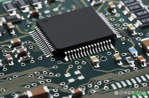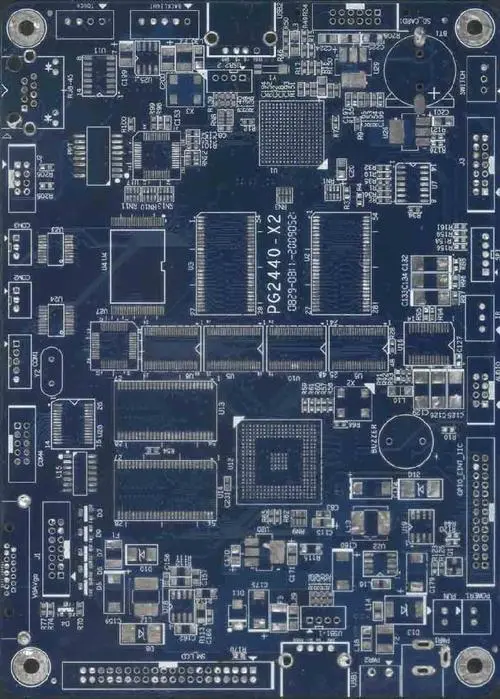
With the development of electronic industry, the integration of PCB electronic components is getting higher and higher, and the volume is getting smaller and smaller. BGA packaging is widely used. Therefore, PCB circuits will become smaller and smaller, and the number of layers will increase. To reduce line width and line spacing is to use a limited area as much as possible, and to increase the number of layers of PCB thin lines is to use space. The main line of the circuit board in the future will be 2-3 mil or less.

It is generally believed that every time a circuit board is added or a grade is added, it must be invested once, and the investment capital is relatively large. In other words, high-end PCB boards are produced by high-end equipment. However, not every enterprise can afford large-scale investment, and it takes a lot of time and money to carry out trial production to collect PCB technology data after investment. It seems to be a better way to carry out experiment and trial production according to the current situation of the company, and then decide whether to invest according to the actual situation and market conditions. This paper describes in detail the limit of thin line width that can be produced under normal equipment conditions, as well as the conditions and methods of PCB production.
The general production process can be divided into acid etching method for covering holes and pattern electroplating method, both of which have advantages and disadvantages. The circuit obtained by acid etching method is very uniform, which is conducive to impedance control, and has less environmental pollution, but a hole fracture will lead to scrapping; Alkali corrosion production is easy to control, but the line is uneven and the environment is polluted.
Circuit board
First of all, dry film is the main material for PCB circuit production. Different dry films have different resolutions, but they can usually display a line width of 2mil/2mil after exposure. The resolution of ordinary exposure machine can reach 2mil, usually here. Lineweight and line spacing within the range do not cause problems. For developer nozzles with a linewidth of 4 mils/4 mils or greater, the pressure and concentration of the drug solution are not very relevant. Below 3mil/3mil linewidth, the nozzle is the key to resolution. Fan nozzle is usually used, and the pressure is about 3BAR.
Although the exposure energy has a great impact on the circuit, most of the dry films used in the market now have a wide exposure range. It can be distinguished in 12-18 levels (25 level exposure scale) or 7-9 levels (21 level exposure scale). Generally speaking, lower exposure energy is conducive to resolution, but when the energy is too low, dust and various impurities in the air can be distinguished. It has a great impact on it, and will cause open circuit (acid corrosion) or short circuit (alkali corrosion) in the subsequent process. Therefore, the actual production should be combined with the cleanliness of the darkroom, so as to select the minimum line width and line spacing of the circuit board that can be produced according to the actual situation.
The smaller the line, the more obvious the influence of development conditions on the resolution. When the circuit is higher than 4.0mil/4.0mil, the development conditions (speed, syrup concentration, pressure, etc.) have no significant effect; When the circuit is 2.0mil/2.0/mil, the nozzle shape and pressure play a key role in the normal development of PCB circuit. At this time, the development speed may be significantly reduced, and the drug concentration will affect the appearance of the circuit. The possible cause is the high pressure of the sector nozzle. When the distance between the lines is small, the momentum can still reach the bottom of the dry film. Therefore, it can be developed; The pressure of conical nozzle is small, so it is difficult to form thin lines. The orientation of the additional plate has a significant effect on the resolution and the side wall of the dry film.
Different exposure machines have different resolutions. At present, one type of exposure machine is air-cooled surface light source, and the other is water-cooled point light source. Its nominal resolution is 4 mil. But the experiment shows that you can reach 3.0mil/3.0mil without special advertisement


