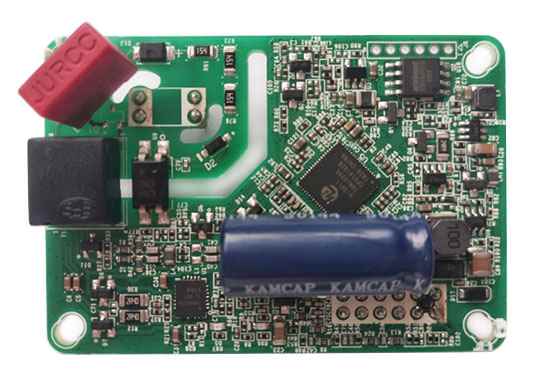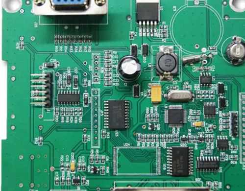
Shenzhen kingford is a professional PCBA manufacturer with its own PCB board factory and SMT patch processing factory. We can provide PCB design, PCB board making, component purchasing, SMT patch, DIP plug-in, PCBA testing, finished product assembly and other one-stop PCBA processing services. Next, introduce pcba processing matters needing attention.
PCBA needs to be considered when manufacturing
1. Design of automatic production line veneer transmission and positioning elements
For automated line assembly, PCbas must have the ability to transmit edges and optically locate symbols, which is a prerequisite for production.
2. PCBA assembly process design
Component layout structure on the front and back of PCBA determines the process method and path of assembly.
3. Component layout design
The position, direction and spacing of components on the assembly surface are designed. The Layout of components depends on the welding method used, and each welding method has specific requirements for the placement, orientation, and spacing of components.
4. Assembly technology design
Oriented to the design of straight through rate of welding, through the matching design of welding pad, welding resistance and steel mesh, the stable allocation of welding paste quantity and fixed point is realized. Through the design of the layout and wiring, the synchronous melting and solidification of all solder joints in a single package are realized. Through the reasonable connection design of the mounting hole, to achieve 75% tin penetration rate, etc., these design goals are ultimately in order to improve the welding yield.

PCBA welding link points for attention
1. Warehouse management personnel should wear anti-static gloves when issuing materials and testing IQC, use instruments to be grounded reliably, and the working table should be laid with anti-static rubber pads in advance.
2, in the process of operation, the use of anti-static workbench, at the same time with anti-static containers for components and semi-finished products. Department welding equipment can be grounded, electric soldering iron must be antistatic type, all equipment must be tested before use.
3. When PCBA is processed in the furnace, due to the scouring of the pin of the plug-in component by tin flow, some plug-in components will be tilted after welding in the furnace, resulting in the element body beyond the screen frame, so it is required to repair welding personnel after the tin furnace to correct it properly.
4, PCBA in the welding horn and battery need to pay attention to solder can not be too much, can not cause the peripheral components short circuit or fall off.
5. PCBA substrates must be neatly placed. Bare substrates cannot be stacked directly. To stack stacks, pack them in electrostatic bags.
PCBA finished product assembly precautions
1. Use an ESD bag for the system without a shell
Periodically test ESD tools, Settings, and materials to ensure that they meet requirements.
2. When assembling finished products, follow the following procedures
Warehouse → production line → upgrade software of production line → Assemble into complete machine →QC test → write IMEI number → full QA check → restore factory Settings → warehousing; The software should be upgraded before assembly. It is not allowed to upgrade the software after assembling the finished machine. It may be unable to upgrade due to improper welding short circuit, working process problems and so on, leading to misjudgment of poor PCBA.
2. High speed high density PCB design company
In the case of fixed circuit board size, if the PCB design needs to accommodate more functions, it is often necessary to improve the PCB wire density, but this may lead to enhanced mutual interference of the wire, at the same time, the impedance can not be reduced, then Shenzhen PCB design company -kingford to introduce high speed and high density PCB design skills.
High speed and high density PCB design skills
In the design of high speed and high density PCB, crosstalk interference should be paid special attention to, because it has a great impact on timing and signal integrity.
Note for high speed and high density PCB design:
1. Control the continuity and matching of the characteristic impedance of the cable.
2. Cable spacing. It is often seen that the spacing is twice the width of the line. Through simulation, we can know the influence of line spacing on timing and signal integrity, and find out the minimum tolerable distance. Different chip signals may have different results.
3. Select an appropriate terminal mode.
4. Avoid routing cables in the same direction or even overlapping on the upper and lower floors. This is because the cross-talk is greater than that on the same floors.
5. Use blind/buried via to increase cabling area. But the production cost of PCB board will increase.
It's really hard to get exactly parallel and equal length in practice, but try to do it anyway. In addition, differential and common-mode terminations can be reserved to mitigate the impact on timing and signal integrity.
Why do you choose kingford for PCBA processing?
1. Strength guarantee
▪SMT workshop: We have imported SMT machines and several sets of optical inspection equipment, with a daily output of 4 million. Each process is equipped with QC personnel, who can keep an eye on product quality.
▪DIP production line: We have two wave-soldering machines, among which there are more than 10 old employees who have worked for more than three years. The skilled workers can weld all kinds of plug-in materials.
2. Quality assurance, cost-effective
▪ High-end equipment can stick precision shaped parts, BGA, QFN, 0201 materials. Can also template patch, loose material hand.
▪ Sample and size batch can be produced, proofing from 800 yuan, batch 0.008 yuan/point, no start-up fee.
3. Rich experience in SMT and welding of electronic products, stable delivery
▪ Accumulated SMT SMT processing services for thousands of electronic enterprises, involving many kinds of automotive equipment and industrial control motherboard. The products are often exported to Europe and the United States, and the quality can be affirmed by new and old customers.
▪ On time delivery, normal 3-5 days after complete materials, small batch can also be expedited on the same day shipment.
4. Strong maintenance ability and perfect after-sales service
▪ Experienced maintenance engineers can repair all kinds of patch welding caused by bad products, to ensure the connection rate of each piece of circuit board.
▪ 24-hour customer service staff at any time response, the fastest speed to solve your order problems.


