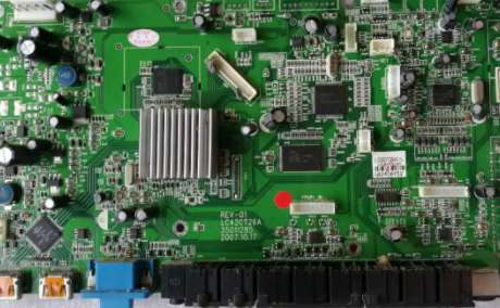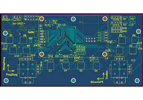
PCB surface treatment is the key and foundation of SMT patch quality. The processing process of this link mainly includes the following contents. Today, Shenzhen SMT factory -kingford would like to share with you the experience we have accumulated in the process of professional PCB proofing.
First, coating thickness in addition to ENG, there is no clear provision in the PC related national standards, only to meet the weldability requirements, the industry can generally require the following.
OSP:0.15~0.5μm, IPC does not specify. 0.3 to 0.4um is recommended
EING: Ni-3 ~ 5um; Au-0.05 ~ 0.20um (PC only specifies the current thinnest can be required)
Im-Ag: 0.05~0.20um thicker, more serious corrosion (not specified for PC)
Im-Sn: ≥0.08um. The reason why we want it thicker is mainly because Sn and Cu will continuously develop into CuSn at room temperature, which will affect the weldability.
HASLSn63Pb37, generally between 1 and 25um natural formation, the process is difficult to accurately control, and lead-free mainly used SnCu alloy, due to high processing temperature, easy to form Cu3Sn sound welding poor, basically not used at present.
2. Wettability of SAC387 (wetting action time under different furnace times, unit: s).
0 times :im-sn(2)floridaageing(1.2), osp(1.2)im-ag(3).
ZweiterPLENARSESSIONZweiterPLENARSESSIONIm - Sn corrosion resistance is best, but the welding resistance is bad!
4 times: ENG (3) -- ImAg (4.3) -- OSP (10) -- ImSn (10).
3. Wettability of SAC305 (after passing through the furnace twice).
ENG (5.1) -- Im-Ag (4.5) -- Im-Sn (1.5) -- OSP (0.3).
In fact, for these professional parameters we do not understand will be very confused, but if it is necessary for SMT patch manufacturers to pay attention to.
Advantages of PCB products:
Energy production from 2 layers to 14 layers, 14-22 layers can be proofing production.
Minimum line width/spacing: 3mil/3milBGA Spacing :0.20MM
Minimum aperture: 0.1mm Size :610mmX1200mm
Ink: Tamura, Taiyo, Fudoken;
FR4: Shengyi, Kingboard, Harbour, Hongren, Guoji, Hezheng, Nanya,
(Shengyi S1130/S1141/S1170),Tg130℃/ Tg170℃ T g180℃ and other high TG plates)
High frequency plate: Rogers, Taconic, ARLLON;
Surface process: tin spray, lead-free tin spray, gold plating, full plate gold plating, plug gold plating, full plate thick gold, chemical tin (silver), anti-oxidation (OSP) blue glue, carbon oil.

2. Complete seven steps of PCBA project
kngford is a professional PCBA manufacturer with its own PCB board factory and SMT patch processing factory. We can provide PCB design, PCB board making, component purchasing, SMT patch, DIP plug-in, PCBA testing, finished product assembly and other one-stop PCBA processing services. Here are seven steps to a successful PCBA project.
First, the preliminary preparation stage
1. PCBA project specification, technical parameters and requirements;
2. Prepare the project lead team, responsible for process design, process implementation, project report and other work;
Ii. Design and development
The criteria for this process is the ability to design circuits that conform to the smt production process.
3. Design and edit operation instruction of SMT production process
1. Clear the format of the working instruction, which is consistent with the PCBA processing plant;
2. Clear operation instructions (solder paste selection operation instructions, steel mesh use operation instructions, patch processing operation instructions, re-flow welding process control instructions, etc.);
Four, steel mesh production capacity confirmation
1, steel mesh production process;
2. Gerber files suitable for steel mesh production are exported from PCB files to guide the process of steel mesh production;
V. Confirm the programming and operation ability of the SMT machine
1. Evaluation of BOM list and Gerber documents;
2. Planter programming, PCB size measurement and plate processing;
Vi. PCBA assembly test
1. SMT patch testing after production (aging, burning, signal, high and low temperature, ICT testing, etc.);
2, three anti paint coating, etc. (three anti refers to which three anti, please refer to our previous analysis of the problem);
Vii. PCBA patch project improvement and evaluation
1. PCBA design mutual inspection;
2. Report;
3. Suggestions for improvement.
Why kingford?
1. Strength guarantee
▪SMT workshop: We have imported SMT machines and several sets of optical inspection equipment, with a daily output of 4 million. Each process is equipped with QC personnel, who can keep an eye on product quality.
▪DIP production line: We have two wave-soldering machines, among which there are more than 10 old employees who have worked for more than three years. The skilled workers can weld all kinds of plug-in materials.
2. Quality assurance, cost-effective
▪ High-end equipment can stick precision shaped parts, BGA, QFN, 0201 materials. Can also template patch, loose material hand.
▪ Sample and size batch can be produced, proofing from 800 yuan, batch 0.008 yuan/point, no start-up fee.
3. Rich experience in SMT and welding of electronic products, stable delivery
▪ Accumulated SMT SMT processing services for thousands of electronic enterprises, involving many kinds of automotive equipment and industrial control motherboard. The products are often exported to Europe and the United States, and the quality can be affirmed by new and old customers.
▪ On time delivery, normal 3-5 days after complete materials, small batch can also be expedited on the same day shipment.
4. Strong maintenance ability and perfect after-sales service
▪ Experienced maintenance engineers can repair all kinds of patch welding caused by bad products, to ensure the connection rate of each piece of circuit board.
▪ 24-hour customer service staff at any time response, the fastest speed to solve your order problems.


