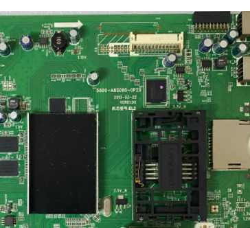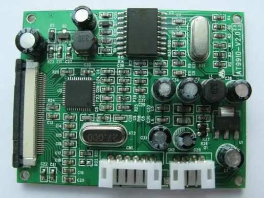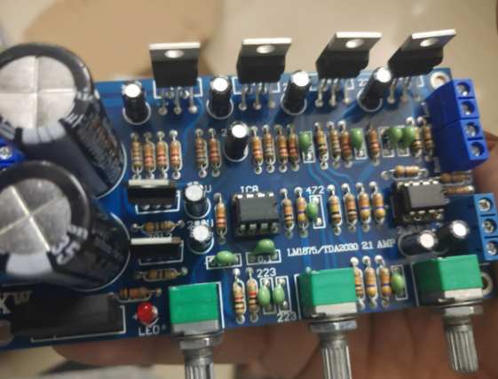
Obviously, any form of PCBA machining welding must have enough solder where it is needed and not cause problems (short circuits, solder balls, spikes, etc.). This is the minimum requirement of PCBA processing.
However, we want to exceed the minimum as much as possible to achieve maximum quality assurance. We need a complete 360° welded connection with no clearance between the opening of the lead and the pad. For electroplating through holes, the material shall fill the electroplating holes vertically and completely. Although most standards allow for less than ideal conditions, the forces that control the flow of solder can be understood and used to achieve 100% perfection.
Factors that determine perfect wave soldering in PCBA processing include:
1. Stabilize full contact
Weld between crests, PCB and component leads.
Step 2: Heat
There are several aspects to this. First, the SMT plant shall dissipate the solvent and activate the flux (deoxidize the surface to be welded) before the component enters the welding wave. The heat is supplied by a heater under the conveyor belt. Next, in the simple case of a single-sided PCB (i.e. there is no plating in the through-hole and therefore no upward flow of solder is required), the solder temperature must be high enough so that the solder does not freeze before opening the hole. The conference has gone out of fashion. Finally, for components with electroplated through-holes, the temperature at the top of the PCB must be higher than the melting temperature of the solder to prevent the solder from freezing before the holes are completely vertically filled.
For decades, the preheater was located just below the conveyor belt. Another heat source (solder tank) is also located below the conveyor belt. For heavier PCBS or components with larger thermal mass, solder will only be held long enough to fill through holes if the conveyor speed is very slow and/or solder temperature is higher than necessary. Prolonged contact with the heating element may scorch the PCB, and too high a soldering temperature will produce more scum, deteriorate the machine parts faster, and cause the PCB to sag or layer.

For almost all modern parts, heaters above and below the parts are essential. The more power the top preheater provides, the less heat is needed at the bottom. Except for components with very heat-sensitive bodies (long ago, bodies made of polyethylene were not uncommon), the top of the PCB was heated to 300°F or (occasionally) higher before the wave worked properly. Even for parts with low melting points, placing a heat shield on the part usually provides adequate protection.
The term "cold welding" is very common in electronic products at the PCBA processing plant in Shenzhen. In most cases, "cold" solder is actually caused by a failure to remove oxides (i.e., in other words, not wetting) rather than a lack of heat. (The British equivalent term is always the more accurate "dry" solder joint.) Incomplete vertical filling of plating holes due to solder freezing is a phenomenon that may properly be called "cold solder". The solution is the top preheater.
3. Separation speed of PCB and welding wave
The slower separation provides more opportunity for excess solder to flow back into the tin tank.
2. Composition of PCBA processing quotation
Before 2010, in terms of the quotation composition of the electronic processing industry we were in contact with, it was mainly SMT processing, which was relatively simple, basically processing fees and testing fees. After this is mainly the PCBA OEM one-stop service, including the whole circuit board processing process, the corresponding quotation composition is more complex, the need to evaluate the content is much more complex than before. Basically, we have the following parts:
PCBA processing cost = PCB cost + steel mesh cost + smt link cost + assembly cost + testing cost.
PCBA processing cost of each part of the introduction
1.PCB cost: The main cost evaluation items of this link are the number of PCB layers, material, process, whether or not the gold finger, size, quantity, welding pad requirements and other special requirements.
2. Cost of steel mesh: Steel mesh is mainly used for solder paste printing in the patch processing link, its importance is self-evident, its printing quality can directly determine whether the welding of SMD components is qualified. At present, steel mesh is mainly divided into etched steel mesh and laser steel mesh, because of the difference in accuracy, there is also a big difference in price. In addition, kingford will keep the used steel mesh free of charge for 3 months, and then if the customer has the demand of return order, it can be reused according to the assessment situation.
3. Component cost: This cost is for the components provided by kingford when customers need them. The quotation sheet given by the supply chain manager will contain the exact quotation of each component, and the customer will evaluate which components we provide and which components we do not need to provide.
4. Assembly cost: The price of this link is mainly affected by the number of SMT patches, the number of DIP or (THT) and other factors. Overall, the quotation evaluation of this link is the fastest.
5. Testing cost: this link is mainly to consider the labor hours and test fixture, auxiliary materials, and the corresponding testing equipment needs to be equipped with loss, etc.
Why do you choose kingford for PCBA processing?
1. Strength assurance
▪ SMT workshop: We have imported SMT machines and a variety of optical testing equipment, capable of producing 4 million pieces per day. Every process is equipped with QC personnel who can keep a close eye on product quality.
▪ DIP production line: There are two wave welding machines. Among them, there are more than ten old employees who have worked for more than three years. Skilled workers can weld all kinds of insert materials.
2. Quality assurance, high cost-effective
▪ High-end equipment can mount precision heterosexual parts, BGA, QFN, 0201 materials. Proofing can be machine paste, also can be hand pendulum.
▪ Samples and large and small batches can be produced. Proofing starting price 800 yuan, batch starting price 0.008 yuan/point, no start-up fee.
3. Rich experience in SMT and welding of electronic products, stable delivery time
▪ Has served thousands of home appliance subsidiaries, involving various kinds of automotive equipment and industrial control motherboard SMT SMT processing services. Products are often exported to Europe and the United States, the quality of new and old customers affirmed.
▪ On time delivery, usually within 3-5 days after the board is assembled, small batch expedited can also be shipped on the same day.
4. Strong maintenance ability and perfect after-sales service
▪ Experienced maintenance engineers are able to repair defective products caused by various welding problems and ensure the connectivity rate of each circuit board.
▪ 24-hour customer service staff will be ready to respond and resolve your order as soon as possible.


