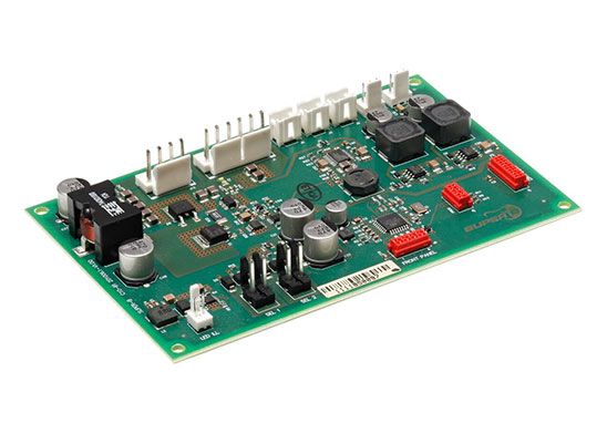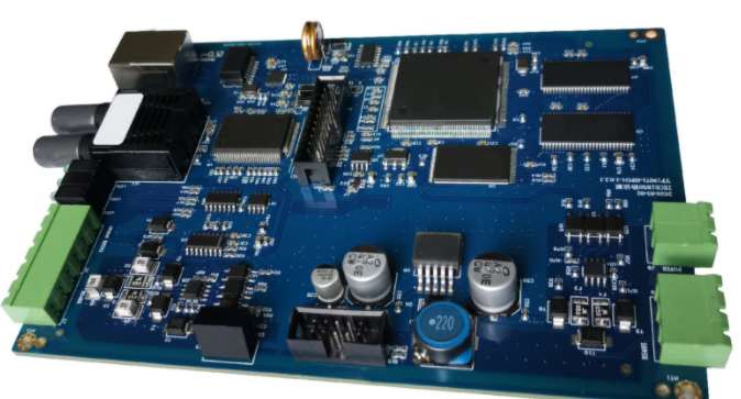
With the rapid development of mobile phone, electronics, communication industry, autonomous driving and other high-tech industries, to a large extent led to the growing and rapid growth of the circuit board industry, people for the quality of the circuit board, the number of layers, weight, precision, materials, color, reliability and other requirements are increasingly high.
Also due to the fierce price competition in the market, the cost of circuit board materials is also on the rise. In order to improve the core competitiveness of the industry, more and more manufacturers choose to try to monopolize the market at low prices. However, these ultra-low prices are often obtained through reducing the cost of materials and process production costs, which leads to the quality of the circuit board itself can not reach, so the circuit board is usually prone to cracks (cracks), easy scratches, (or bruises), its precision, performance and other comprehensive factors did not reach the standard, seriously affecting the reliability of the circuit board, Should prove that cheap no good goods, but good goods must not be cheap is an ironproof fact, in the face of a variety of circuit board manufacturers on the market, how to distinguish the quality of the circuit board from the appearance, the next professional Circuit board manufacturer -kingford for you to introduce.
Distinguish the circuit board is good or bad method
In general, the circuit board can be judged by the appearance of several aspects;
1. Light and color.
External PCB circuit boards are covered with ink, circuit boards can play the role of insulation, if the color of the board is not bright, less ink, insulation board itself is not good.
2, PCB circuit board size and thickness of the standard rules.
The thickness of the circuit board to the standard circuit board is different sizes, customers can measure and check according to their own product thickness and specifications.
3. Appearance of PCB circuit board weld.
Due to more parts of the circuit board, if the welding is not good, parts easy to fall off the circuit board, seriously affect the welding quality of the circuit board, good appearance, careful identification, the interface is very important.

2. What are the requirements of PCB board for SMT processing
SMT processing, usually PCB board has a lot of requirements, and must meet the requirements of the board to accept SMT welding processing. Then, why SMT welding process needs to have so many requirements on the circuit board?
It has been proved that in the SMT process, there will be a lot of special processes, and the application of special processes will immediately bring the requirements for PCB board. If there are problems with PCB board, it will increase the difficulty of PCBA welding process, which may eventually lead to welding defects, unqualified boards and other situations. Therefore, in order to ensure the smooth completion of the special process and facilitate SMT processing, PCB board must meet the manufacturability requirements in dimensions, pad distance and other aspects.
SMT processing requirements for PCB board are as follows:
1. PCB size
The width of the PCB (including board edges) must be greater than 50mm and less than 460mm, and the length of the PCB (including board edges) must be greater than 50mm. If the size is too small, it needs to be assembled.
2, PCB board edge width
Edge width > 5mm, plate spacing < 8mm, distance between plate and edge > 5mm.
3. PCB bending degree
Upward curvature: < 1.2mm, downward bending: < 0.5mm, PCB deformation: maximum deformation height ÷ diagonal length < 0.25.
4, PCB board Mark point
Mark shape: Standard circle, square, triangle
Mark size: 0.8~1.5mm
Mark materials: Gold, tin, copper and platinum
Mark's surface requirements: smooth surface, no oxidation, no dirt
Requirements around Mark: Within 1mm of the mark, there should be no obstacles such as green oil, which is obviously different from the color of the mark
Mark position: More than 3mm away from the edge of the plate, and no marks such as holes and test points shall be found within 5mm
5. PCB welding pad
There is no through hole on the patch component pad. If there is a through-hole, the solder paste will flow into the hole, resulting in less tin in the device, or the tin flow to the other side, resulting in uneven surface, unable to print solder paste.
When designing and manufacturing PCB, it is necessary to know some knowledge of PCB welding process in order to make the product suitable for production. Understanding the requirements of the processing plant first can make the subsequent manufacturing process more smooth and avoid unnecessary trouble.
This is the SMT processing of PCB board requirements, in the production of PCB board is not slack, the production of high-quality compliant PCB board can better let the board accept other special technology, and give PCB board life, and inject the soul of function.
kingford PCB board advantages:
Energy production from 2 layers to 14 layers, 14-22 layers can be proofing production.
Minimum line width/spacing: 3mil/3milBGA Spacing :0.20MM
Minimum aperture: 0.1mm Size :610mmX1200mm
Ink: Tamura, Taiyo, Fudoken;
FR4: Shengyi, Kingboard, Harbour, Hongren, Guoji, Hezheng, Nanya,
(Shengyi S1130/S1141/S1170),Tg130℃/ Tg170℃ T g180℃ and other high TG plates)
High frequency plate: Rogers, Taconic, ARLLON;
Surface process: tin spray, lead-free tin spray, gold plating, full plate gold plating, plug gold plating, full plate thick gold, chemical tin (silver), anti-oxidation (OSP) blue glue, carbon oil


