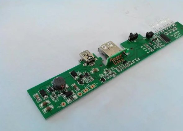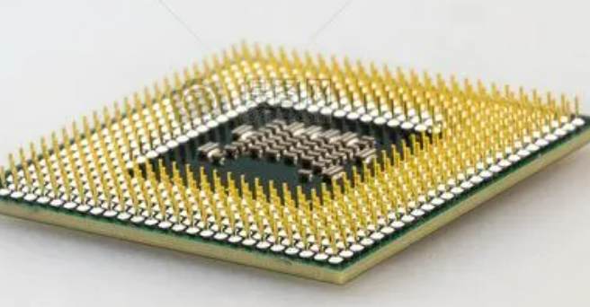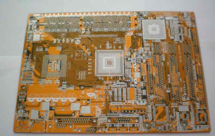
In the SMT processing process, the circuit board reflow welding will warpage, which will cause the component welding, tablet and other defects. Next, Shenzhen PCBA processing manufacturer kingford will introduce how to avoid the warpage of PCB board in PCBA processing.
PCBA machining to avoid PCB board warping method
1. Reduce the influence of temperature on the stress of the plate
Since the temperature is the main source of the stress of the board, the warping of PCB board can be greatly reduced by reducing the temperature of the backwelding furnace or slowing down the heating and cooling speed of the board in the backwelding furnace. But there may be other side effects, such as a short circuit in the solder.
2. High Tg plate is used
Tg is the glass conversion temperature, that is, the temperature at which the material changes from glass state to rubber state. The lower the Tg value is, the faster the board will become soft after entering the backwelding furnace, and the longer it will take to become soft rubber state, the more serious the deformation of the board will be. The plate with higher Tg can increase its ability to withstand stress and deformation, but the price of the material is relatively high.
3. Increase the thickness of the circuit board
Many electronic products in order to achieve the purpose of thinner, the thickness of the board has been left 1.0mm, 0.8mm, and even 0.6mm thickness, such a thickness to keep the board in the welding furnace without deformation, really a bit of force, it is suggested that if there is no light and thin requirements, the board can use the best thickness of 1.6mm, It can greatly reduce the risk of warping and deformation of PCB board.
4. Reduce the size of the circuit board and reduce the number of boards
Since most backwelding furnaces use chains to drive the circuit board forward, the larger the size of the circuit board will sag and deform in the backwelding furnace because of its own weight, so try to put the long side of the circuit board as the board side on the chain of the backwelding furnace, you can reduce the weight of the circuit board caused by the sag deformation, reduce the number of plates is also based on this reason, That is to say, when the furnace, as far as possible to use the narrow side of the vertical direction of the furnace, can achieve the lowest depression deformation.
5. The tray fixture has been used
If the above methods are difficult to do, the last is to use the furnace tray (reflow carrier/template) to reduce the deformation of the circuit board, looking for components on the spot only sample store furnace tray fixture can reduce the PCB board warpage principle is because the fixture material will generally choose aluminum alloy or synthetic stone with high temperature resistance characteristics, Therefore, after the high-temperature expansion of the circuit board in the backwelding furnace and the cold contraction after cooling, the tray can play the function of stabilizing the circuit board. When the temperature of the circuit board is lower than the Tg value and begins to recover and harden, the original size can still be maintained.
If a single layer of tray fixture can not reduce the deformation of the circuit board, it is necessary to add a layer of cover, the circuit board with two layers of tray clip up, so that you can greatly reduce the circuit board over the welding furnace deformation problem. But the trays are expensive, and you have to add labor to place and retrieve them.
6. Use the Router instead of the V-Cut
Since V-cuts can damage the structural strength of the board, try not to use V-Cut subboards, or reduce the depth of the V-Cut.

2. How do PCB design companies do silkscreen design well?
Many people who draw PCB will think that screen printing does not affect the performance of the circuit, so they do not pay attention to screen printing. However, professional PCB design engineers must pay attention to these details. Next, kingford, Shenzhen PCB design company, will introduce how to do a good silkscreen design.
How to do screen printing design in PCB design?
1. The location of the display
Generally speaking, the screen printing of resistance, capacitance, pipeline and other devices should not be placed in four directions, so that when debugging, maintenance, welding screen printing will lead to fatigue (the board to rotate in several directions).
Therefore, it is recommended that they be placed in both directions, as shown in the figure below. Silkscreen printing would then be looked at in a very different way.
How to do screen printing design in PCB design?
If the components are too dense to place a silkscreen, you can write a silkscreen, mark arrows, and draw a box in the nearby blank for easy identification.
How to do screen printing design in PCB design?
2. Try not to hit the screen printing through the hole
3, screen printing do not press on the high-speed signal line (such as, clock line, etc.)
This recommendation applies to high speed signal lines on top or bottom layers, as such signal lines can be considered microstrip lines.
The speed (phase velocity) of the signal running on the microstrip line is dependent on the medium. If the silk screen is pressed onto a straight line, the medium will become uneven, resulting in a change in phase velocity, and ultimately the impedance is discontinuous, affecting the quality of the signal.
Of course, the signal line of the internal electrical layer will not have this problem.
4. The reading direction of screen printing should be consistent with the direction of use
The direction of reading the screen print is the same as the direction of using the chip, mainly to reduce the probability of backwelding during welding.
Others, such as electrolytic capacitors, also cannot follow this recommendation because positive and negative polarity can be indicated.
5. The pin number should be marked clearly on the screen printing
As shown in the following figure, there are four pin numbers on the P3 connector for easy debugging/installation. Also, it is best to mark locations with dense pins, such as chips, FPC sockets, etc.
At the same time, it is also in line with previous suggestions. The reading direction of P3 is the same as that of the connector.
kingford is a professional PCB design company engaged in electronic products layout layout design, mainly undertake multi-layer, high density PCB design and circuit board design proofing business. Proficient in the use of market mainstream PCB design software, professional and efficient communication to ensure the progress of PCB design, to help you seize the market opportunity one step earlier!


