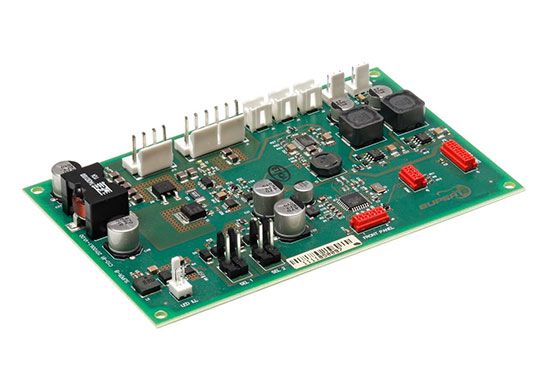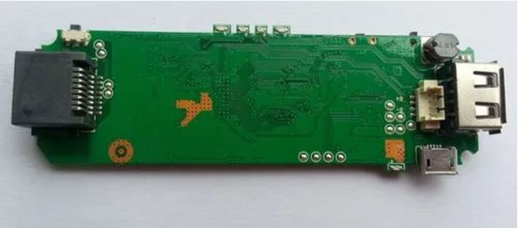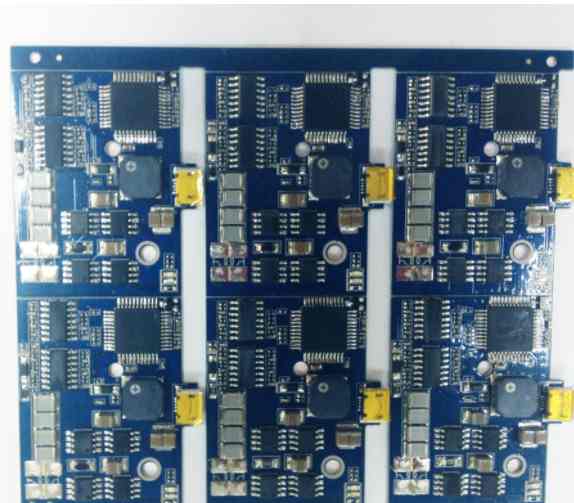
PCB board is a complex process, in PCB board a series of production processes, a lot of matching points, not careful board will have defects, involved in the whole body, PCB quality problems will emerge in endlessly, such as the common short circuit, open circuit and so on, Next, Shenzhen PCB board manufacturer -kingford will introduce the common bad causes of PCB board.
Common bad reasons for PCB board making
1. Short circuit
(1) Improper pad design, we can change the circular pad to oval, increase the distance between points, prevent short circuit.
(2) Improper direction design of PCB parts, for example, if the SOIC foot is parallel to the tin wave, it will cause short circuit, so we can appropriately modify the direction of the part, so that it is perpendicular to the tin wave.
(3) The bending foot of automatic plug-in will also cause PCB short circuit. Because the length of the pin is less than 2mm stipulated by IPC, and the parts will fall off when the Angle of the bending foot is too large, it is easy to cause short circuit. Therefore, it is necessary to leave the welding spot more than 2mm away from the line.
In addition to the above 3 points, there are also some reasons that will cause short circuit problems of PCB board, such as the hole of the substrate is too large, the tin furnace temperature is too low, the weldability of the board surface is not good, the welding resistance film failure, the board surface is polluted and so on. Engineers can conduct a series of troubleshooting according to the above reasons.
2. Open circuit
An open circuit occurs when the trace breaks, or when the solder is only on the pad and not on the component lead.
This is because there is no adhesion or connection between the component and the PCB, just like a short circuit, which can occur during manufacturing or welding and other operations.
Vibrating or stretching circuit boards, dropping them, or other mechanical deformation factors can damage the trace or solder joints.
Chemical or moisture can cause solder or metal parts to wear out, which can cause component leads to break.
3. Dark and granular contacts appear on the PCB board
This kind of problem on PCB board is mostly because solder is polluted and dissolved tin mixed with too much oxide, resulting in too brittle solder joint structure. Care should be taken not to confuse the dark color with the use of low tin content solder.
Another reason for this problem is that the solder itself used in the process of processing and manufacturing changes, the content of impurities is too much, the need to add pure tin or replace the solder.
Physical changes in the fibril deposition of stained glass, such as the separation of layers.
But this is not a bad solder joint, but the substrate is too hot, reduce the preheating and solder temperature or increase the substrate speed.

4, PCB board solder joints become golden
Normally, the solder of PCB board is silver gray, but occasionally there are golden solder spots. The main reason for this problem is that the temperature is too high, at this time only need to lower the temperature of the tin furnace.
5. Environmental impact
In extreme temperature or temperature change, humidity is too large, high intensity vibration and other environments, it is easy to cause damage to PCB board. For example, changes in ambient temperature can cause the board to deform, which can break solder joints, bend the shape of the board, or cause copper wires on the PCB board to break.
The moisture in the air will lead to oxidation, corrosion and rust on the metal surface, such as exposed copper wire, solder joints, pads and component leads will be affected to a certain extent.
Accumulation of dirt, dust, or debris on the surface of the components and PCB board can reduce air flow and cooling of the components, resulting in overheating and degraded performance of the PCB.
Vibration, dropping, hitting or bending the PCB will cause it to deform or crack, while high current or overvoltage will lead to breakdown of the PCB board or rapid aging of components and pathways.
Shenzhen kingfordPCB board ability
Energy production from 2 layers to 14 layers, 14-22 layers can be proofing production.
Minimum line width/spacing: 3mil/3milBGA Spacing :0.20MM
Minimum aperture: 0.1mm Size :610mmX1200mm
Ink: Tamura, Taiyo, Fudoken;
FR4: Shengyi, Kingboard, Harbour, Hongren, Guoji, Hezheng, Nanya,
(Shengyi S1130/S1141/S1170),Tg130℃/ Tg170℃ T g180℃ and other high TG plates)
High frequency plate: Rogers, Taconic, ARLLON;
Surface process: tin spray, lead-free tin spray, gold plating, full plate gold plating, plug gold plating, full plate thick gold, chemical tin (silver), anti-oxidation (OSP) blue glue, carbon oil
kingford Electronics is a Circuit board manufacturer specializing in the manufacture of printed circuit boards, 20 years focused on single, double-sided, multi-layer circuit board production. We can provide PCB proofing and mass production services such as FR4 hard board, FPC soft board, HDI board and metal substrate.


