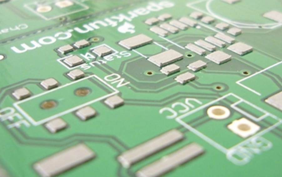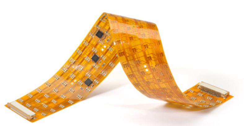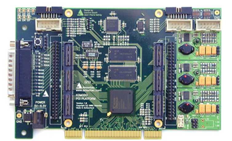
The characteristics of the mixed packaging process are: on one side of the PCB board (side A has a number of IC components, and inserted through hole components, on the other side of the PCB (side B) and there are many patch resistance capacitance electrical parts (sometimes IC), often called "mixed packaging". It retains the advantages of cheap through hole components, common in audio-visual products, such as CD, DVD.
The operation process of the mixed loading process is: using solder paste - reflow welding process to weld IC components on side A; Coated with patch glue on side B and sent to infrared furnace curing; Then turn to side A and insert the through-hole component; Wave welding B side; PCB arrangement, cleaning, testing, assembly.
The ultimate purpose of bonding SMD/SMC on the PCB circuit board is to weld, but only the components are bonded on the PCB (excluding all bonding defects), and it cannot guarantee that the SMA can be welded well through wave soldering. This is because chip components have almost no leads, and SMC/SMD has its particularity in wave soldering.
During wave soldering of through-hole components, the lead wire of the components contacts the high temperature solder wave and under the action of flux, the wetting force will promote the solder to extend the lead wire to climb up, so as to wet the whole pad and get a good welding effect. For example, if the holes on PCB are metal holes, the solder can also extend through the metal holes to the other side of the PCB and form a full solder spot.

However, the chip device is directly bonded on the PCB because there is no pin, and the surface of the component and circuit board forms an acute Angle, so that the flowing solder wave impacts the surface of the resistance and capacitor along the tangential direction, and it is not easy to reach the corner formed by the rectangular component and PCB plane, and it becomes more obvious with the increase of the thickness of the original. In this corner, it is easy to gather the bubbles formed by flux and flux residue, resulting in welding leakage or poor welding. People often refer to this corner as the "welding dead zone."
Another problem of patch-wave soldering is that the end welding head of chip components is usually SnPb coated, which has good weldability. In order to ensure the smooth PCB, the surface is usually coated with gold plating or preheating flux, which is not as effective as SnPb alloy hot air smoothing process. When passing through the solder wave, the wetting time of the two is not the same. Usually, the SnPb end electrode is only 0.1s, while the copper layer needs 0.5s. The end of the component first contacts with the solder, so it is also easy to cause "welding dead zone". In order to solve the defect of "welding dead zone", double wave wave welding technology is usually adopted, that is, pulse wave is added to make the solder wave impact the "welding dead zone" in the vertical direction, so as to achieve good welding effect.
In addition, low solid flux should be used to reduce residue in the dead zone; Increase PCB preheating temperature to improve weldability; Improve the component arrangement direction and reduce the dead zone corner to reduce the bad spot rate.
Therefore, in the wave soldering of SMC/SMD components, the direction of component arrangement should be strictly considered in PCB design. As far as possible, the direction of component pins should be perpendicular to the direction of motion during wave soldering. IC components should be placed on side A of PCB as far as possible, less on side B, and must be placed on side B. The auxiliary pad should also be increased. The activity and density of flux are also requirements that cannot be ignored. In addition, the curing strength of components should meet the requirements, especially the residual glue should not be bonded on the pad.


