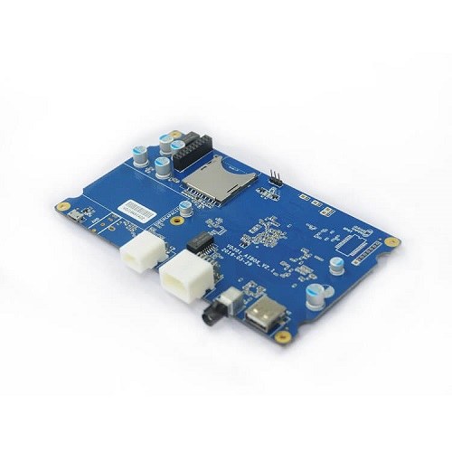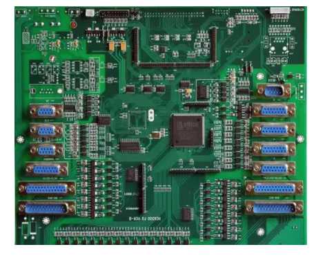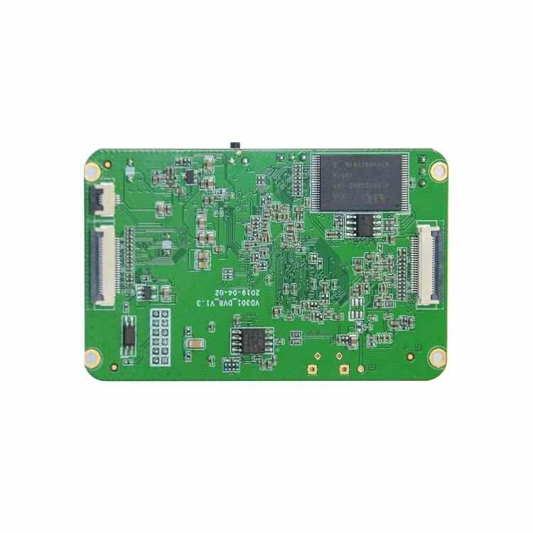
Why is there a defect in wave soldering of PCB pad? The following SMT factorywill give you an analysis of the causes and solutions.
①PCB design is unreasonable and the spacing between pads is too narrow.
(2) The pins of the plug-in components are irregular or skewed, and the pins are close to or have met before welding.
(3) PCB preheating temperature is too low. During welding, components and PCB absorb heat, which reduces the actual welding temperature.
④ The welding temperature is too low or the speed of the conveyor belt is too fast, so that the viscosity of the molten solder is reduced.
⑤ Poor flux activity.
SMT patch processing
Therefore, our solutions are:
First, design according to the PCB design specification.
The pin of the second cartridge component shall be formed according to the hole spacing and assembly requirements of the PCB.
Third, set the preheating temperature according to PCB size, board layer, number of components, whether there are attached components, etc., PCB bottom temperature is 90 ~ 130℃.
The fourth tin wave temperature is (250±5) ℃, and the welding time is 3 ~ 5s. When the temperature is slightly lower, the conveyor speed should be slowed down.
Fifth, replace the flux.
Common PCB pad over wave soldering defects have the following points:
(1) The board surface is dirty. This is mainly due to the high solid content of the flux, too much coating, preheating temperature is too high or too low, or due to the transfer of mechanical claw is too dirty, solder pot oxide and tin slag too much.
(2) PCB deformation. Generally, it occurs on large-size PCB, because large-size PCB has high quality or uneven Layout of components, resulting in unbalanced quality. This requires PCB design as far as possible to make components distributed evenly, in the middle of the large size PCB design process edge.
(3) drop (drop) the piece. The quality of the patch adhesive is poor, or the curing temperature of the patch adhesive is incorrect, the curing temperature is too high or too low will reduce the bonding strength, wave soldering can not withstand the effect of high temperature impact and wave shear force, so that the mounting components fall in the material pot.
(4) Other recessive defects. Solder joint grain size, solder joint internal stress, solder joint internal crack, solder joint brittle, solder joint strength is poor, need X-ray, solder joint fatigue test and other detection. These defects are mainly related to welding materials, adhesion of PCB pad, weldability of components' welding ends or pins, temperature curves and other factors.

2.PCB flying needle online test technology
For printed circuit boards that cannot be tested using a needle bed, a flying needle on-line tester can be used. During the test operation, according to the pre-programmed coordinate position program, the test probe is moved to the test point to contact with it, and each test probe carries out on/short circuit test or component test on the assembled components according to the test program.
Flying needle type online tester is installed with a number of needles, each needle is installed at the appropriate Angle, will not occur test dead Angle phenomenon, can carry out all-round Angle test. Therefore, the fly - needle on - line tester can greatly improve the bad detection rate.
Generally, the test program of flying needle online tester is automatically generated. The method is as follows: PCB circuit CAD system is connected with test equipment to form a data link station, the position coordinates of CAD data output are transformed into probing coordinates, and then the test program is produced from node data and component data. The CAD data can be directly converted into the test program, which can greatly reduce the programming time and reading cycle, and reduce the operation cost.
PCBA processing
(1) PCB label positioning. By means of the wiring reference label on the printed circuit board and the coordinate correction based on image recognition, the fabrication errors of the measured circuit board and the setting errors of the circuit board can be reduced, so as to achieve high precision measurement.
The function principle of image recognition and position correction of the reference label is as follows: the CCD camera reads the reference label printed on the printed circuit board wiring, the image processing device extracts the center coordinates of the mark, calculates the offset with the reference coordinates, and then corrects the X-Y coordinates programmed in advance for measurement.
(2) The selection of probe shape and the selection sequence of test points.
① Selection of probe shape. The probe contact points of the surface mounted circuit board have different types of test line, through hole, component pin, etc. The probe of the flying needle type online tester can choose the most appropriate probe shape according to the requirements.
② The selection sequence of test points. The test points can be selected in the following order: test point, chip pad with spacing above 2125, IC pin pad with spacing above 0.8mm, through hole (when components exist), bare hole, chip pad with spacing below 1608 (but specify 2 points), IC pin pad with spacing below 0.65mm.


