PCBA machining requirements for plug-in hole design?
Plug-in processing is a process of PCBA processing. The processing of plug-in components generally adopts wave soldering. Because the wave soldering time is very short, if the jack is connected to more ground/electric layers, the tin penetration will be poor, resulting in poor welding.
pcba process requirements for plug-in hole design
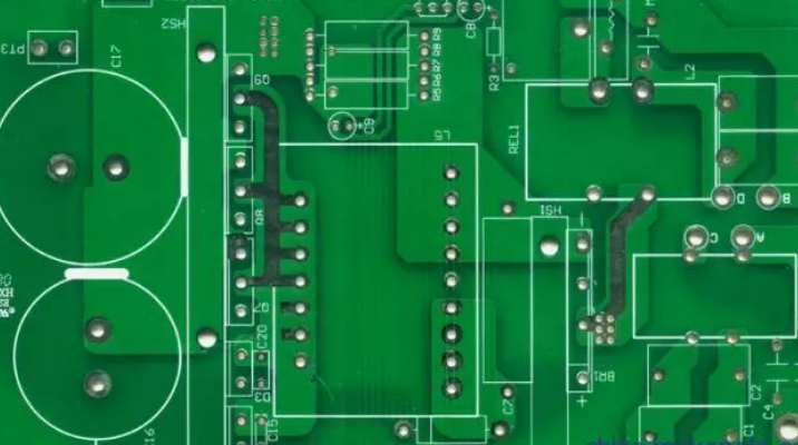
1. In order to ensure the tin penetration rate in the plug-in hole, it is generally recommended that the hole and the inner layer of the ground/electrical layer adopt the design of flower welding pad, and the specific size of pcba processing technology can refer to the relevant standards. If a real connection is used, it is recommended to limit it to two layers.
2. If the circuit design needs to carry large current, it must meet certain requirements of carrying capacity. In PCBA processing process, it is recommended to adopt the design of power holes, that is, the plug-in holes can realize the needs of carrying capacity through the surface solder joints and power holes, and the number of power holes is designed according to the load capacity.
Power hole
3. In order to meet the design requirements of more than 20A load capacity, pcba processing technology is conditionally allowed to connect strata to four layers. Requirements: Four layers are close to the PCB heating surface, that is, two layers are close to the welding surface, two layers are close to the component surface, and the component surface can be heated.
4. If four layers of ground/electrical layer are connected, but the face of the pin component is covered by the packaging body, the pcba processing technology must adopt the power hole design.

DIP plug-in processing process of wafer processing plant
With the rapid development of SMT processing technology, SMT patch processing has gradually replaced DIP insert processing. However, due to the large size of some electronic components in PCBA production, plug-in processing has not been replaced and still plays an important role in the process of electronic assembly processing. DIP plug-in processing is after SMT patch processing, generally using pipelined manual plug-in, requiring a lot of staff.
The DIP plug-in processing process can be generally divided into: component forming processing → plug-in → over-wave soldering → component cutting → repair welding (post welding) → plate washing → function testing
1. Preprocessing components
First of all, the staff in the preprocessing workshop will go to the material department to get the materials according to BOM, carefully check the type and specification of the materials, sign the materials, and preprocess according to the samples before production. They will use the automatic bulk capacitance clipper, automatic transistor forming machine, automatic belt forming machine and other forming equipment for processing.
2. Plug-in
Insert the machined components into the corresponding position of the PCB board to prepare for over-wave soldering.
3. Wave soldering
Put the plug-in PCB board into the wave soldering conveyor belt, and complete the welding of PCB board after spraying flux, preheating, wave soldering, cooling and other steps.
4. Component cutting feet
Cut the feet of the welded PCBA board to achieve the appropriate size.
5. Repair welding (post welding)
The finished PCBA plate that is not completely welded should be repaired and repaired.
6. Wash the board
Clean the flux and other harmful substances left on PCBA products to achieve the environmental cleanliness standard required by customers.
7. Functional testing
Functional testing shall be carried out on the finished PCBA board after the components are welded to test whether each function is normal. If functional defects are found, maintenance and re-testing shall be carried out.
smt patch is short for a series of processes based on PCB. PCB (printed circuit board) means printed circuit board. (Text: smt patch refers to the short PCB (Printed Circuit Board) for a series of processes processed on the basis of PCB.)
SMT (short for Surface Mounted Technology) is the most popular technology and process in the electronic assembly industry. Surface Mount Technology (SMT) of electronic circuits is called surface mount or surface mount technology. It is a pin-free or short-lead surface assembly components (SMC/SMD, Chinese known as chip components) installed on the surface of the Printed Circuit Board (PCB) or other substrate surface, through reflow welding or immersion welding and other methods to be welded and assembled circuit installation technology.
Under normal circumstances, the electronic products we use are designed by pcb plus various capacitors, resistors and other electronic components according to the designed circuit diagram, so all kinds of electrical appliances need a variety of smt SMT processing technology to process.
SMT basic process elements: solder paste printing -> Parts mounting --> Reflow welding --> AOI Optical Detection --> Maintenance --> The board is divided.
Some people may ask why it is so complicated to connect an electronic component. In fact, this is closely related to the development of our electronic industry. Nowadays, electronic products pursue miniaturization, and the previously used punch plug-in components can not be reduced. Electronic products function more complete, the integrated circuit (IC) used has no perforated components, especially large scale, high integration IC, have to use surface patch components. Product mass, production automation, the factory to low cost and high output, produce quality products to meet customer needs and strengthen the market competitiveness of the development of electronic components, integrated circuit (IC) development, semiconductor material multiple applications. Electronic science and technology revolution is imperative, chasing international trends. It can be imagined that the development of smt surface assembly technology and process is inevitable in the case that intel,amd and other international manufacturers of cpu and image processing devices have improved their production process to more than 20 nanometers.
smt patch processing advantages: high assembly density, small size of electronic products, light weight, the size and weight of the patch components is only about 1/10 of the traditional plug-in components, generally after the adoption of SMT, the size of electronic products reduced by 40%~60%, 60%~80% weight reduction. High reliability and strong vibration resistance. Low defect rate of solder joint. Good high frequency characteristics. Electromagnetic and radio frequency interference is reduced. Easy to realize automation, improve production efficiency. Reduce the cost by 30%~50%. Save materials, energy, equipment, manpower, time, etc.


