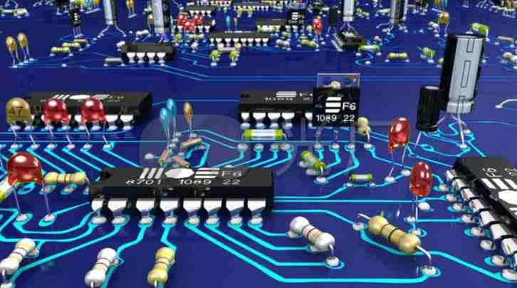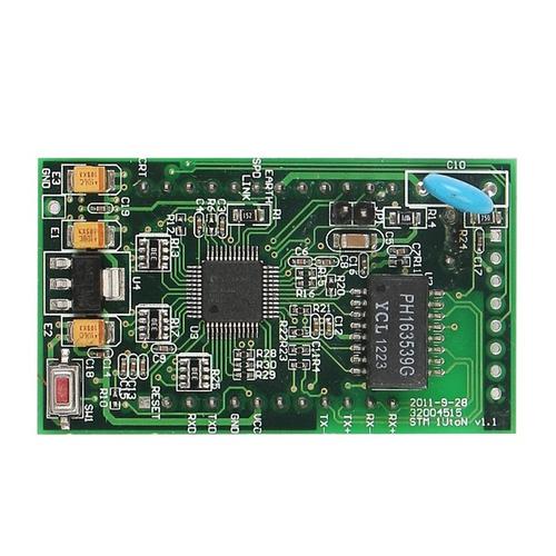
Generally, PCB board proofingwill be done for testing before doing experiments or mass production of PCB board. There are many forms of pcb files. In order to meet different market needs, pcb board manufacturers can open these different forms of files. Then, what materials need to be prepared before pcb board proofing? Follow long Bo technology to understand!
In general, pcb or GERBER files should be provided to pcb manufacturers for pcb board proofing. The provided files should include some board making instructions, such as the number of sub-layers of the board, required material, pad process, ink color and other specific Production requirements. Specific instructions are as follows:
1. Materials: To explain what materials are needed to produce pcb, FR4 is commonly used, and the main material is epoxy resin stripped fiber cloth board.
2. Board layer: After pcb board proofing, the number of layers has an impact on the price, so it is necessary to indicate how many layers of board to be made.
3. Welding resistance color: the conventional color is green, other colors need to be indicated.
4. Screen printing color: screen printing font and frame color on pcb board, the default choice is generally white.
5, copper thickness: generally according to the current of pcb board circuit to scientifically calculate the thickness of copper, generally the thicker the better, but the cost will be higher, so the need for a reasonable balance.
Whether the hole is covered by solder resistance: The solder resistance is to insulate the hole, otherwise it is to let the hole is not insulated.
6, surface coating: pcb board before proofing to explain the surface coating is spray tin or gold plating.
7. Quantity: The quantity of pcb should be clearly stated.
At present, the production of pcb circuit board is mostly reduced method, that is, the excess copper foil on the raw material copper coated plate is subtracted to form conductive graphics. The method of subtracting is to use chemical corrosion, economic and efficiency is relatively high. Only chemical corrosion has no differential attack, so it is necessary to protect the required conductive pattern, coating a layer of corrosion inhibitor on the conductive pattern, and then the unprotected copper foil corrosion.

What is the normal 6-layer pcb circuit board production process? Long bo technology and share!
1. Make two non-porous double-sided pcb circuit boards first
Cutting (raw material double-sided copper clad)- Inner graphic making (form graphic resist)- Inner etching (subtract excess copper foil)
2. The two made inner pcb core boards are bonded and pressed together with epoxy glass fiber semi-cured sheets
Riveted the two inner core pcb boards and the semi-cured sheet, and then placed a copper foil on each outer side of the press under high temperature and high pressure to complete the pcb board pressing, so that the adhesion. The key material is semi-cured sheet, which has the same composition as the original material and is also an epoxy resin glass fiber, but it is not fully cured and will liquify at 7-80 ° C. Among them, pcb circuit board is added with curing agent, and it will cross-link and solidify with resin at 150 ° C, and then it will be no longer reversible. By this semi-solid - liquid - solid transformation, adhesion is achieved under high pressure.
3, conventional double panel production
Drilling - electroplating copper plate (hole metalization)- outer circuit (forming graphic resist layer)- outer etching - welding resistance (printing green oil, text)-pcb board surface coating (tin spraying, gold plating, etc.)- forming (milling forming), complete!
With the continuous development of electronic products, the frequency of various equipment failures is greatly increased, and the requirements for maintenance personnel are also constantly improving, especially for the maintenance personnel who just contact the circuit board. Many people do not know how to start at the beginning, and do not know how to learn. In fact, if you want to learn the maintenance of pcb board well, you need several electrical and modular electrical foundations.
pcb board schematic blueprint, the realization of the circuit user needs the function. The design of pcb board mainly refers to the design of the layout, the need for internal electronic components, metal wiring, through hole and external connection layout, electromagnetic protection, heat dissipation, crosstalk and other factors.
The following points should be paid attention to when repairing pcb board:
1. Before maintenance, first of all, we should do a good job of preventing static electricity, such as wearing clothes and shoes to prevent static electricity and wearing a wrist strap to prevent static electricity. The maintenance table should also be done to prevent electrostatic treatment, such as to prevent electrostatic table.
2, pay attention to electricity, including the circuit board to take into account the bearing capacity of the pcb circuit board.
3, when you need to contact strong electricity, pay attention to the human body, do a good job of strong electricity prevention measures.


