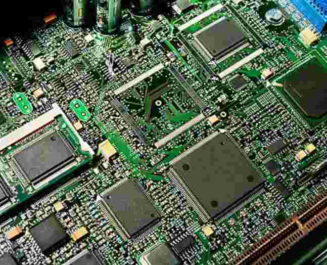
Appearance consideration: the appearance of PCB circuit board module should be close to square, the width × length of the module should be less than 125mm×180mm, and the outer frame (clamping edge) of the PCB module should adopt closed-loop design to avoid deformation after the pcb module is fixed on the fixture.
<!--[if !supportLists]-->1. <!--[endif]-->After opening V-shaped slots, the remaining thickness X shall be (1/4 ~ 1/3) plate thickness L, but the thickness X shall be ≥0.4mm. The upper limit is recommended for the board with a heavy load, and the lower limit is recommended for the board with a light load. For the thickness of the plate less than 1.2mm, it is not suitable to use V-slot plate.Mark point: Set the reference anchor point. The reference anchor point is required to be surrounded by an open weld area 1.5mm larger than it.
Process edge: There should be no large device or protrude device near the connection point between the outer frame of the splinter board and the inner small board, and the small board and the small board, and the edge of the component and PCB circuit board should be more than 0.5mm space, to ensure the normal operation of the cutting tool.

printed circuit boards save manufacturing costs
In order to keep the cost of PCBS as low as possible, a number of factors must be taken into account:
The size of the board is, of course, important. The smaller the board, the lower the cost. Part of the PCB size has become the standard, as long as the size then the cost will naturally fall. The Custom PCB website has some information about standard sizes.
Using SMT is cheaper than using THT because the PCB will be more densely packed (and smaller).
On the other hand, if the parts on the board are dense, the wiring must also be finer, and the equipment used is relatively higher order. At the same time, the material used should also be more advanced, and the design of the wire must be more careful, so as not to cause power consumption and other problems affecting the circuit. These problems cost more than the savings from shrinking PCBS.The more layers, the higher the cost, but a PCB with fewer layers usually results in an increase in size.

Drilling takes time, so as few pilot holes as possible.
Burials are more expensive than pilot holes that run through all layers. Because burials have to be drilled before they can be joined.The size of the hole in the board is determined by the diameter of the pin of the part. If the board has parts with different types of pins, then the machine cannot use the same drill bit to drill all the holes, the relative time consumption, also represents a relative increase in manufacturing costs.
Electronic tests using a fly pin probe are usually more expensive than optical tests. In general, optical testing is sufficient to ensure that there are no errors on the PCB.
In short, manufacturers are getting more and more sophisticated with their equipment. It is useful to know the manufacturing process of PCBS because when comparing mainframe boards, boards of the same performance may have different costs and different stability, which allows us to compare the capabilities of different manufacturers.Good engineers can look at the main board design, know the quality of the design. You may think you're not that strong, but the next time you get your hands on a console board or display card, you might want to take a look at the beauty of PCB design.
How to improve the SMT patch processing efficiency?

First, prepare for work in advance.Due to the particularity of PCBA process, SMT must be the first process. At the same time of the first processing procedure, the cooperation degree of various departments is also one of the keys to ensure the SMT patch processing efficiency. Including the accurate output of the entire processing process documents, the accuracy of component procurement, the accuracy of component inspection, material preparation, program editing, solder paste thawing, components baking, etc. These are the preparation of the work in advance, rather than in the actual production process to do or confirm. It can avoid as many problems as possible outside the actual production and processing, which also solves the time of online abnormal processing, and indirectly improves the efficiency of SMT patch processing. Advance preparation work and SMT plant management process has a lot to do with.
2. Ensure the running time balance of SMT mounter


