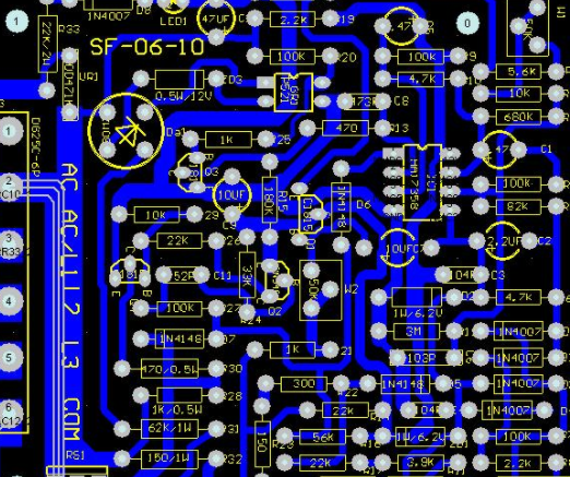
How to solve the problem of PCBAfaulty soldering
What is PCBA faulty soldering? It means that the surface appears to be welded, but there is no connection inside, or it is in an intermediate unstable state that may or may not be connected. This is the most abominable. It is difficult to find problems. It is often called cold solder. Some are caused by poor welding or lack of tin, which causes the element foot and the welding pad to be disconnected. Others are caused by oxidation or impurities of the element foot and the welding pad, which is really difficult to see with the naked eye. Generally, it is caused by oxidation or impurities at welding points, poor welding temperature and improper methods.
Essentially, there is an isolation layer between the solder and the pin. They are not completely in contact with each other, and their state cannot be seen by the naked eye. However, their electrical characteristics are not conductive or poorly conductive Influence circuit characteristics. PCBA faulty soldering is a common kind of circuit fault. There are two kinds. One is an unstable state caused by improper production process in the process of PCBA production; The other is caused by the aging and peeling of the solder joint at the weld leg of some parts with severe heat after long-term use of the appliance. The components must be stored in a moisture-proof way. The in-line components can be slightly polished. During welding, solder paste and flux can be used. It is better to use a reflow soldering machine. Manual soldering should be technically good. As long as the first welding is good, there is generally no false welding. "After long-term use of electrical appliances, the solder joints at the weld legs of some parts with severe heat are prone to aging and peeling" This is a bad foundation.
Solution to PCBA faulty soldering:
1) Determine the approximate fault range according to the fault phenomenon. 2) Appearance observation, focusing on larger components and components with large heat. 3) Observe with a magnifying glass. 4) Pull the circuit board. 5) Shake the suspected component by hand, and observe whether the pin solder joint is loose. PCB company has its own PCB board factory and SMT chip processing factory, which can provide one-stop services for PCB manufacturing, component purchasing, DIP plug-in processing, SMT chip processing, and PCBA function testing!

How to Layout and Route BGA Devices
PCB company has a professional PCB design team with an average working experience of more than 10 years, and can skillfully use mainstream PCB design software. Welcome friends who have PCB layout design needs to come to consult! Next, I will introduce the layout and wiring skills of BGA devices in PCB design. With the rapid development of electronic products towards portable/miniaturization and networking, higher requirements are put forward for electronic assembly technology, among which BGA (Ball Grid Array Package) is a high-density assembly technology that has entered the practical stage. The research of BGA technology started in the 1960s and was first adopted by IBM in the United States. But it was not until the early 1990s that BGA really entered the practical stage. Due to the previously popular high-density pin devices similar to QFP package, the limitation of its fine spacing is that thin leads are easy to bend, brittle and break, and the requirements for coplanarity and mounting accuracy between leads are very high. BGA technology adopts a new design thinking mode. It adopts a structure that hides round or cylindrical points under the package, with large lead spacing and short lead length. In this way, BGA eliminates the defects of coplanarity and warpage caused by lead wire problems in fine pitch devices. BGA is a commonly used component on PCB, usually 80% of high-frequency signals and special signals will be pulled out from this type of packaging Footprint. Therefore, how to handle the routing of BGA devices will have a great impact on important signals. How to route BGA devices? When wiring ordinary BGA devices, the general steps are as follows:
1. First, determine the number of boards required according to the number of bonding pads of BGA devices, and then conduct the stack design.
2. Then fan out the main device BGA (that is, lead a small segment of line from the pad, and then place a via at the end of the line, so that the via can reach another layer).
3. Then escape wiring from the via to the edge of the device, and fan out through the available layers until all pads are escape wiring completed. The cabling during fanout and escape is carried out according to the applicable design rules.
It includes fanout control fanout control rule, wiring width RouTing Width rule, wiring via method RouTing Via Style rule, wiring layer RouTing Layers rule and electrical clearance rule. If the rules are set unreasonably, for example, the number of layers is not enough, the unlimited width is too wide to walk out, the through-hole is too large to drill, the spacing violates the safety distance, etc., the fan out will fail. When the fanout operation does not respond, please check your rule settings and make appropriate modifications. Fanout can succeed only after there are no problems. As shown in the figure below. The routing color of each layer is different. The Fan Out dialog box allows you to control and define the options related to fan out and escape routing, and some options are used for blind holes (holes between layer pairs can be set in the Layer Stack Manager dialog box of the stack manager). Other options include whether the other two rows and columns are fanned out at the same time as the internal rows and columns, and whether only the pads assigned to the network are fanned out. How to wire extremely small BGA (0.4mm spacing) devices? Because of the complexity of BGA's processing technology, in addition to its functional design, the most important thing in the design phase is to communicate with PCB manufacturers and chip assembly plants. Different manufacturers have different processes and capabilities. For processing and manufacturing costs, proofing and batch production are also different. Therefore, more importantly, BGA design should also consider the processing cost, the yield rate of production and other factors.
Today's BGA is not a fuel saving lamp. This kind of BGA module design has refreshed the bottom line and belongs to the category of minimum processing capacity. Let's take a look at its parameter characteristics: the BGA pad is 0.3mm (12mil), and the BGA center spacing is 0.4mm (16mil). The X and Y directions of the pad and the pad edge to edge are 0.1mm (4mil). The diagonal direction of pad and pad edge is 0.27mm (10.8mil). So here comes the question...! Let's review the previous blog post, "How can rule settings be applied to my pcb design? - - pcb manufacturing line width, line spacing and hole diameter", which introduces the most precise processing capability of pcb processing plants. Now, the screenshots of the main line width, line spacing and aperture limit processing capacity are as follows: Attention! The minimum line width is 0.1mm (4mil), the minimum safe spacing is 0.1mm (4mil), and the minimum laser aperture is 0.1mm (4mil). We don't think about mechanical drilling, and the laser hole can't be put down!


