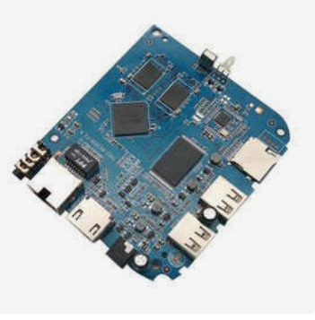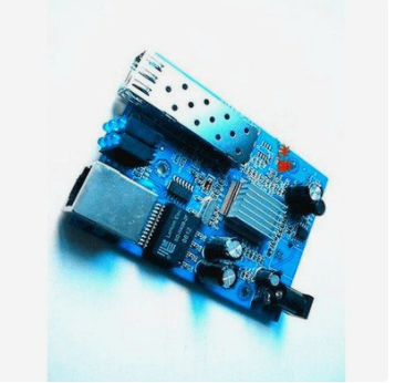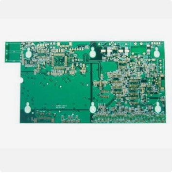
The following is about the application advantages of low ㎡ UV laser in PCB technology in microelectronic materials in PCB manufacturing:
Mobile devices such as smartphones and tablets are growing rapidly. As mobile devices become smaller and smaller, faster and faster, lighter and lighter, cheaper and more functional, and more complex, the manufacturing of parts is also developing towards miniaturization and precision. For some key components, such as semiconductor chips, microelectronic packages, touch screens and printed circuit boards (PCBs), they will continue to face challenges, such as improving yield and productivity, while reducing costs. This has promoted the wide application of lasers in mobile device manufacturing. Due to the increasing complexity of equipment, more and more complex manufacturing processes are required, and higher requirements are put forward for the research progress of laser light sources.

A laser with shorter wavelength and pulse width and lower M2 (beam quality) can create a more focused spot, and maintain the minimum heat affected zone (HAZ), thus achieving more precise micro machining. With high energy absorption, especially in the ultraviolet (UV) wavelength and short pulse range, the material will be vaporized rapidly, thus reducing the heat affected zone and carbonization. Smaller focus spot can realize machining with higher precision and smaller size. High power, high pulse repetition rate (PRF), pulse shaping and pulse splitting can all contribute to improving the productivity of micromachining. The continuous high pulse stability ensures the repeatability of the process and helps to achieve higher yield.
The traditional UV Q-switched diode pumped solid state (DPSS) lasers can reasonably meet the requirements of precision manufacturing, but they are still lacking in achieving higher processing speed and higher micro processing quality. The common method to improve the processing speed is to increase the pulse repetition rate of the laser while keeping other process parameters unchanged. However, this is impossible for a typical Q-switched DPSS laser. The average power and pulse energy of these lasers will decrease rapidly with the increase of pulse repetition frequency. In addition, when the pulse repetition rate is high, the laser pulse width and pulse energy fluctuation often increase significantly.
This paper combines high power and independently adjustable UV laser pulse width and advanced pulse regulation technology at high pulse repetition rate, and applies them to the micromachining of various microelectronic materials, including silicon (application in chip manufacturing), aluminum oxide (application in microelectronic packaging manufacturing) Glass (application in touch screen manufacturing) and copper (application in printed circuit board and microelectronic packaging manufacturing).
Silicon Marking in semiconductor manufacturing
Laser cutting silicon wafer can replace traditional precision sawing. As the chip becomes thinner and thinner, and the laser becomes more powerful, the advantages of laser are further enhanced compared with sawing. In order to compete with traditional sawing, it is essential to achieve higher scoring speed and better cutting quality.
We use Quasar laser to measure the thickness less than 100 μ M polished single crystal silicon wafer for high-speed marking with minimum thermal damage. In Figure 1, the curve shows that with the increase of the scoring speed, the scoring depth will decrease (200kHz, 25ns single pulse). Higher power is used at higher repetition rates. At the same time, the TimeShift technology can use software to set a wide range of pulse energy and pulse width. Finally, we can see that the marking speed has been increased by almost three times (25ns single pulse, 50 μ M).
Marking of alumina ceramics
Alumina (Al2O3) ceramics are widely used in microelectronic packaging due to their high dielectric properties, high strength, corrosion resistance, high stability and relatively low cost. In a typical manufacturing process, the large-sized aluminum oxide substrate with multiple modules will eventually be separated into a single module (single module). In the commonly used marking technology ("scratch and break"), the laser is used to make deep scratches on the substrate, and then the substrate is broken and separated by mechanical pressure. High power UV laser can achieve clean and accurate high-speed marking.
Similar to silicon engraving, we can see that when using a Quasar laser to perform alumina engraving at a higher speed, we can use higher power and TimeShift technology to achieve the minimum thermal effect.
Glass cutting in flat panel display
During the manufacturing process of the display, the peeling of the glass blocks of the touch screen and LCD requires straight cutting, while the creation of corners, holes and grooves requires curve cutting. The glass substrate used in consumer electronic products has become thinner and thinner through various chemical or heat treatments, and its strength is also getting higher and higher. Therefore, laser processing of glass shows great potential in achieving high-quality cutting and high productivity, and can also reduce the output loss caused by traditional mechanical engraving and stripping processes.
The TimeShift technology we developed is a technology that uses the interaction between laser and matter to process glass. The PCB technology is being patented. In this technology, modification of a single laser pulse can reduce the heat load and the resulting material fragments or fragments. This can achieve good cutting quality and wire cutting speed of more than 1.5m/s in the cutting of chemically strengthened glass, such as Corning Gorilla glass, Asahi Dragontail glass and Schott Xenation glass. Similar results can be obtained in the processing of soda lime glass and advanced flexible glass (such as Corning Willow glass), while the process development of sapphire processing is also in progress.
Copper Cutting in Advanced Packaging and Interconnection
For the thin (10-20 μ m) Clean and fast cutting of copper layer is a typical application of Flexible circuit board cutting. In addition, the drilling in the PCB structure includes ablation of copper layers of similar thickness. We have studied the potential utility of TimeShift technology in these applications, mainly by using sub pulses (pulse trains) to mark copper to improve the depth of grooves.
Summary
We found that the combination of high power UV laser with high pulse repetition rate and TimeShift programmable pulse shaping technology (Quasar laser) can greatly improve the processing effect of micromachining.
The application of ultraviolet laser to the mass processing of a variety of common microelectronic materials (including silicon, ceramics, glass, copper) can bring many benefits. By expanding the PCB process parameter space (increasing the power at a higher pulse repetition rate), coupled with advanced pulse splitting and shaping technologies, we can improve the processing speed and micro machining quality. Through appropriate parameter optimization, the use of this new UV nanosecond pulse laser source can achieve better quality and higher productivity, thus improving the ability of laser micro processing today, so as to face higher challenges for the manufacturing of consumer PCB products in the future


