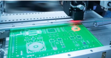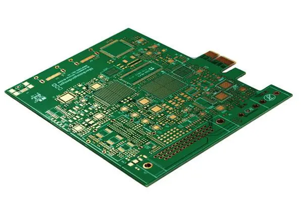
PCB is diversified in materials, layers and manufacturing process to suit different electronic products and their special needs, so there are many types of PCB.
The following summarizes some common ways to distinguish, to briefly introduce the classification of PCB and its manufacturing process. So let's analyze it from three aspects.

A, the material
Material is introduced
From the beginning of the 20th century to the end of the 1940s, PCB substrate material industry is the embryonic stage of development. Its development characteristics are mainly shown in this period of substrate materials used in resin, reinforced materials and insulating substrate emerged in large quantities, technology has been preliminarily explored. These are printed circuit board with the most typical substrate material - coated copper plate appearance and development, create the necessary conditions. On the other hand, the PCB manufacturing technology, which takes the metal foil etching method (reduction method) to manufacture circuit as the mainstream, has been initially established and developed. It plays a decisive role in determining the structure composition and characteristic conditions of the copper clad plate.
Copper clad
Copper clad plate in PCB production was really adopted on a large scale, first appeared in 1947 in the United States PCB industry. PCB substrate material industry has entered its initial stage of development. In this stage, the raw materials used in the manufacture of substrate materials -- organic resins, reinforcement materials, copper foil manufacturing technology progress, the progress of substrate materials industry to give a strong impetus. Because of this, substrate material manufacturing technology began to mature step by step.
The invention and application of integrated circuit and the miniaturization and high performance of electronic products have pushed PCB substrate material technology onto the track of high performance development. With the rapid expansion of the demand for PCB products in the world market, the output, variety and technology of PCB substrate material products have been developed at a high speed. This stage substrate material application, appeared a broad new field - multilayer printed circuit board. At the same time, the structural composition of the substrate materials at this stage has been more diversified.
In the late 1980s, portable electronic products such as laptops, mobile phones, and small video cameras began to enter the market. The rapid development of these electronic products towards miniaturization, lightweight and multi-function has greatly promoted the progress of PCB towards micro hole and micro wire. Under the changing market demand of PCB, a new generation of multilayer board, called laminated multilayer board (BUM), which can realize high-density wiring, was developed in the 1990s. This important technology breakthrough has also enabled the substrate material industry to enter a new stage of development dominated by substrate materials for high density interconnect (HDI) multilayer boards. In this new stage, the traditional copper-clad technology faces new challenges. The PCB substrate material has been changed and created in terms of manufacturing materials, production varieties, organizational structure and performance characteristics of the substrate, as well as in the function of the product.

Second, the finished product soft and hard
1, hard plate: hard plate is a kind of sheet made of PVC as raw material. PVC hardboard is a widely used product in industry, especially in chemical industry.
PVC is a kind of acid, alkali, salt resistant resin, because of its good chemical properties and relatively low price, widely used in chemical, building materials, light industry, machinery and other industries. As shown in figure:
2, soft plate: soft PVC extrusion sheet by PVC resin added plasticizer, stabilizer and other extrusion molding and made.
It can also be used as a general electrical insulation and sealing gasket material. The temperature is -5 to +40℃. It can be used as an alternative product of rubber sheet. As shown in figure:
3, soft and hard combination board: the birth and development of FPC and PCB, gave birth to the soft and hard combination board this new product. Therefore, the combination of soft and hard board, is the Flexible circuit board and hard circuit board, after pressing and other processes, according to the relevant process requirements together, formed with FPC characteristics and PCB characteristics of the circuit board.
Three, the structure
1, single panel: Single panel is the most basic PCB, parts are concentrated on one side, wire is concentrated on the other side. Because the wire is present on only one side, we call this type of PCB single-sided.
Because the single panel had many severe restrictions on the design circuit (because there was only one side, the wires could not be crossed but had to be routed in separate paths), only early circuits used this type of board. As shown in figure:
2, double panel: double panel is including Top (Top) and Bottom (Bottom) both sides are coated with copper printed circuit board, both sides can wire welding, a layer of insulation layer in the middle, for a commonly used printed circuit board.
Both sides can take a line, reduced the difficulty of wiring greatly, because THIS is widely used. As shown in figure:
3, multilayer plate: the production method of multilayer plate is generally made of the inner graph first, and then made of single-sided or double-sided substrate by printing etching method, and incorporated into the specified layer, and then heated, pressurized and bonded, as for the later drilling is the same as the double-panel plating through hole method. As shown in figure:
The above is the classification of PCB from three aspects.


