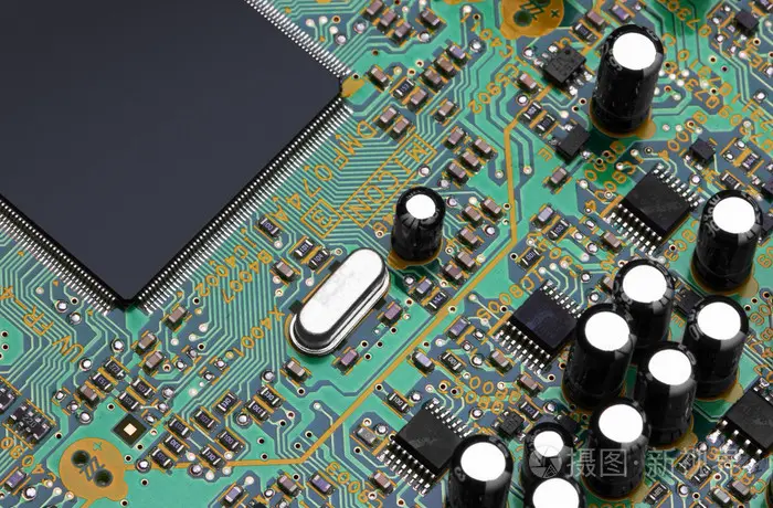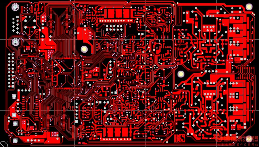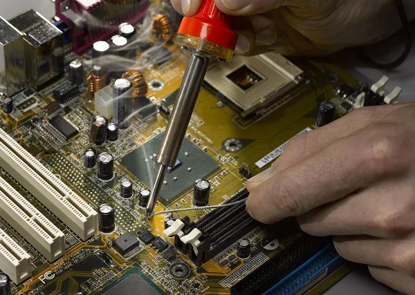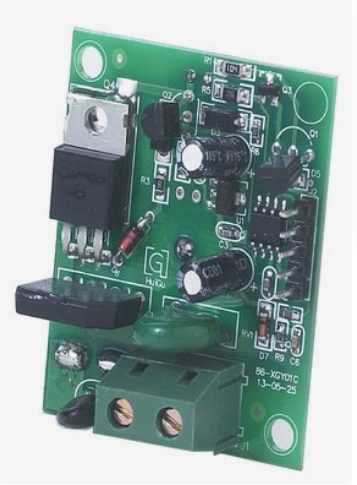
Printed Circuit Board (PCB), also known as printed circuit board in Chinese, is an important electronic component, the support body of electronic components, and the carrier of electrical connection of electronic components. Because it is made by electronic printing, it is called a "printed" circuit board.
PCB board has the following three main types of division:

1. The single panel
Single-sided Boards On the most basic PCB, with parts concentrated on one side and wires on the other (the same side with patch components and the other side with plugins). Because the wire is present on only one side, this PCB is called single-sided. Because the single panel had many severe restrictions on the design circuit (because there was only one side, the wires could not be crossed but had to be routed in separate paths), only early circuits used this type of board.
2. Double panel
Double-sided Boards have wiring on both sides, but to use the wires on each side, you must have a proper circuit connection between them. This "bridge" between circuits is called a pilot hole (VIA). Pilot holes are small, metal-filled, or metal-coated holes in a PCB that can be connected to wires on both sides. Because the area of the double panel is twice as large as that of the single panel, the double panel solves the difficulty of the staggered wiring in the single panel (it can be guided to the other side through holes), and it is more suitable for the more complex circuit than the single panel.
3. A multilayer
To increase the area that can be wired, multilayer Boards use more single - or double-sided wiring Boards. With a double lining, two one-way for outer layer or two double lining, two blocks of single outer layer of the printed circuit board, through the positioning system and alternate insulation adhesive materials and conductive graphics interconnection according to design requirement of printed circuit board becomes four, six layer printed circuit board, also known as multilayer printed circuit board. The number of layers of the board does not mean that there are several independent wiring layers. In special cases, empty layers are added to control the thickness of the board. Usually, the number of layers is even and contains the outermost two layers. Most host boards are 4 to 8 layer structures, but the technical theory can be up to 100 layer PCB board. Most large supercomputers use fairly multi-layered mainframe boards, but since these computers can be replaced by clusters of regular computers, super-multi-layered boards have fallen out of use. Because the layers in the PCB are tightly integrated, it is generally not easy to see the actual number, but if you look closely at the host board, you can still see it.
PCB role
After electronic equipment adopts printed board, due to the consistency of the same type of printed board, so as to avoid the error of manual wiring, and can realize the automatic insertion or placement of electronic components, automatic soldering, automatic detection, to ensure the quality of electronic equipment, improve labor productivity, reduce the cost, and easy to maintain.
PCB Features (Advantages)
PCB is used more and more often because it has many unique advantages, including the following.
It can be high-density. For decades, the high density of printed boards has been able to evolve as integrated circuits become more integrated and installation technologies improve.
High reliability. Through a series of inspections, tests and aging tests, the PCB can be guaranteed to work reliably for a long time (service life, generally 20 years).
Designability. PCB performance (electrical, physical, chemical, mechanical, etc.) requirements, can be designed through standardization, standardization, etc., to achieve the PCB design, short time, high efficiency.
It can be productive. Using modern management, can be standardized, scale (quantity), automation and other production, to ensure product quality consistency.
Testability. A relatively complete test method, test standards, various test equipment and instruments have been established to detect and identify the PCB product conformity and service life.
Assemblability. PCB products not only facilitate the standardized assembly of various components, but also can be automated and large-scale production. At the same time, PCB and various components assembly parts can also be assembled to form larger parts, systems, until the whole machine.
Maintainability. Since PCB products and various component assemblies are standardized in design and scale production, these components are also standardized. Therefore, once the system failure, can be quickly, convenient, flexible replacement, quickly restore service system work. Of course, many more examples could be given. Such as the system miniaturization, lightweight, high-speed signal transmission and so on.
PCB Industry Trends
The PCB industry is growing rapidly
Since the reform and opening up, China's preferential policies in labor resources, market, investment and other aspects have attracted the large-scale transfer of European and American manufacturing industry. A large number of electronic products and manufacturers have set up factories in China, which has driven the development of related industries including PCB. According to the statistics of China CPCA, in 2006, China's actual PCB output reached 130 million square meters, and the output value reached 12.1 billion US dollars, accounting for 24.90% of the world's total PCB output value, surpassing Japan to become the world's first. From 2000 to 2006, the annual growth rate of China's PCB market reached 20%, far exceeding the global average level. The 2008 global financial crisis had a huge impact on the PCB industry, but it did not bring a catastrophic blow to China's PCB industry. Under the stimulus of the national economic policy, China's PCB industry showed a comprehensive recovery in 2010, and the output value of China's PCB reached $19.971 billion in 2010. Prismark expects China to maintain a compound annual growth rate of 8.10 per cent between 2010 and 2015, higher than the global average of 5.40 per cent.
Uneven regional distribution
China's PCB industry is mainly distributed in South China and East China, which together account for 90% of the country, showing obvious industrial aggregation effect. This phenomenon is mainly related to the fact that the main production bases of China's electronic industry are concentrated in the Pearl River Delta and Yangtze River Delta.
PCB downstream application distribution
The downstream application distribution of PCB industry in China is shown in the figure below. Consumer electronics accounted for the highest proportion of 39%; Computers followed, accounting for 22%; Communications 14 percent; Industrial control/medical devices 14%; Automotive electronics 6%; Defense and aerospace accounted for 5 percent.

Outdated technology
Although China has already ranked first in the world in terms of industrial scale, it still lags behind the world advanced level in terms of the overall technological level of PCB industry. In terms of product structure, multi-layer board occupies most of the output value proportion, but most of them are low-end products under 8 layers. HDI and flexible board have a certain scale, but there is a gap between them and Japan and other foreign advanced products in terms of technology content. The IC board with the highest technology content is rarely produced by domestic enterprises.
What are the PCB board quality?
94V-0, 94V-2 belong to a class of flame retardant material, and these two kinds of 94V-0 and belong to the highest flame retardant material. PCB board is generally divided into several colors, green is the most common, and black, red, blue, yellow color and quality is irrelevant, just a personalized performance.
PCB board is mainly considered material and thickness, rarely consider the color. You should be talking about the color of solder resistance ink! Solder resistance ink colors are white, yellow, black, red, blue, and a transparent ink, the most used is green ink. According to the precision of the board used solder ink is different.
It can be divided into organic material and inorganic material
A. Organic materials phenolic resin, glass fiber /Epoxy resin, Polyimide, BT/Epoxy and so on belong to.
B. Inorganic materials
History of aluminum, copper-Invar-copper, Ceramic, etc


