There are more and more electronic devices, and many things are developing in the direction of intelligence, which requires more circuit boards to undertake the control system of these devices. Here is how to choose circuit board processing.
PCBA processing technology
The Method of Choosing PCBA Processing Technology Correctly in PCB Processing
1. Single side
Add solder paste to the component pad. After the solder paste printing of the bare PCB is completed, install its related electronic components through reflow soldering, and then perform reflow soldering.
2. Single side DIP insertion

The PCB board that needs to be inserted is wave soldering after the production line workers insert the electronic components. After the welding is fixed, the feet can be cut and the board can be washed, but the wave soldering production efficiency is low.
3. Single side mixed loading
PCB board shall be printed with solder paste, pasted with electronic components, fixed by reflow soldering, installed with DIP after quality inspection, and then wave soldering or manual soldering. If there are few through hole components, manual soldering is recommended.
4. Single side mounting and plug-in mixing
Some PCB boards are double-sided boards, which are mounted on one side and inserted on the other side. The process flow of mounting and inserting is the same as that of single-sided processing, but fixture is required for PCB reflow soldering and wave soldering.
5. Double sided SMT mounting
In order to ensure the aesthetics and functionality of PCB boards, some engineers will use double-sided mounting. IC components are arranged on side A and chip mounted components are arranged on side B. Make full use of PCB board space to reduce PCB board area.
6. Mixed loading on both sides
There are two methods for double-sided mixed loading:
The first method is that PCBA is processed and assembled for three times with low efficiency, and wave soldering with red glue process has low qualification rate, which is not recommended.
The second method is applicable to the situation where there are many double-sided SMD components and few THT components, so manual welding is recommended. If there are many THT components, wave soldering is recommended.
Complex process of circuit board production
In general, the more complex the functions of electronic products are, the longer the loop distance is, the more contact pins are, and the more layers PCB needs. PCB manufacturers are relatively complex, involving a wide range of processes, from simple machining to complex machining, including ordinary chemical reactions, photochemical electrochemistry, thermochemistry, computer aided design CAM, etc. In addition, there are many process problems in the production process, and new problems are always encountered. Some problems cannot be solved because the process is a discontinuous assembly line. Any problem in any link may lead to the whole line shutdown or a large number of scrapping. If the printed materials are scrapped, they cannot be recycled. The process engineers have a lot of work pressure. Therefore, many engineers leave the industry, Instead, they are engaged in the business of printed circuit board equipment or materials, sales and technical services.
The base material of the plate itself is made of insulating and heat insulating materials and is not easy to bend The visible thin wire is copper foil. The original copper foil is covered with a whole sheet, but it is etched during the manufacturing process. The remaining part becomes a network of thin wires, which are called conductor patterns or wiring. Used to provide circuit connection of components on PCB.
To install the parts on the PCB, we weld its pins directly to the wiring On the most basic PCB (single board), all parts are concentrated on one side, while the wires are concentrated on the other side. In such a case, it is necessary to make holes in the plate. The plate is penetrated in this way to weld the part to the other side, so the connecting part of the part should be welded to the other side. The positive and negative sides of a PCB are called component side and solderside respectively.
If there are some components on the PCB that need to be taken out or reassembled after manufacturing, a socket will be used for the installation of this component. Since the jack is directly welded to the board, the components can be disassembled at will.
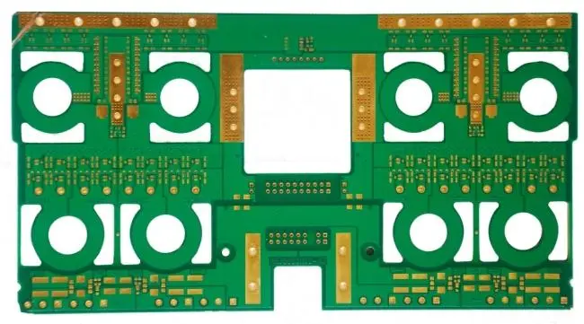
To connect two PCBs to each other, people usually use the edge bonding, which is usually called "gold finger". There are many unexposed copper pads on the gold finger. In fact, such copper pads are also part of PCB wiring. Usually, insert the golden finger on one PCB into the appropriate slot on the other PCB (usually called expansion slot Slot). In a computer, like a display card, sound card or other interface cards, it is connected to the motherboard through the golden finger.
Green or brown on the printed circuit board is the color of soldermask. This layer is an insulating protective layer, which can protect copper wires and prevent components from being welded to the wrong position. An additional layer of silk screen is printed on the solder mask. Usually, words and symbols (mostly white) are printed here to mark the position of parts on the board. The silk screen surface is also known as the "legend".
PCB is made of complex circuit copper wires between components through careful design, etched on a board, making it a basic component for the installation and interconnection of electronic components, and an indispensable basic component in all electronic products.
PCB is a flat plate made of non-conductive materials, on which there are usually pre drilled holes designed to install chips and other electronic components. By electronic means, the hole of the component can make the metal path printed on the board surface connect electronically, then pass through the PCB through the PCB through the PCB pin, and then form a circuit by bonding the conductive metal electrode with the PCB.


